III-nitride transistor epitaxial structure and transistor device

A technology of epitaxial structures and nitrides, which is applied in the manufacture of transistors, semiconductor devices, semiconductor/solid-state devices, etc., can solve the problems of complicated process steps, low threshold voltage of enhanced HEMT devices, unsuitable for production and application, and achieve high electronic efficiency. Mobility, suppression of lateral leakage, and effects of improving crystal quality

Pending Publication Date: 2019-11-26
珠海镓未来科技有限公司
View PDF9 Cites 0 Cited by
  • Summary
  • Abstract
  • Description
  • Claims
  • Application Information

AI Technical Summary

Problems solved by technology

However, the threshold voltage of enhanced HEMT devices obtained by these methods is usually low, and the process steps are complicated, and the reliability still needs to be improved, which is not suitable for a wide range of production and applications.

Method used


Image

  • III-nitride transistor epitaxial structure and transistor device
  • III-nitride transistor epitaxial structure and transistor device
  • III-nitride transistor epitaxial structure and transistor device

Examples


Embodiment Construction

[0021] The present invention will be further described in detail below in conjunction with the accompanying drawings and embodiments. It should be understood that the specific embodiments described here are only used to explain the present invention, but not to limit the present invention. In addition, it should be noted that, for the convenience of description, only some structures related to the present invention are shown in the drawings but not all structures.

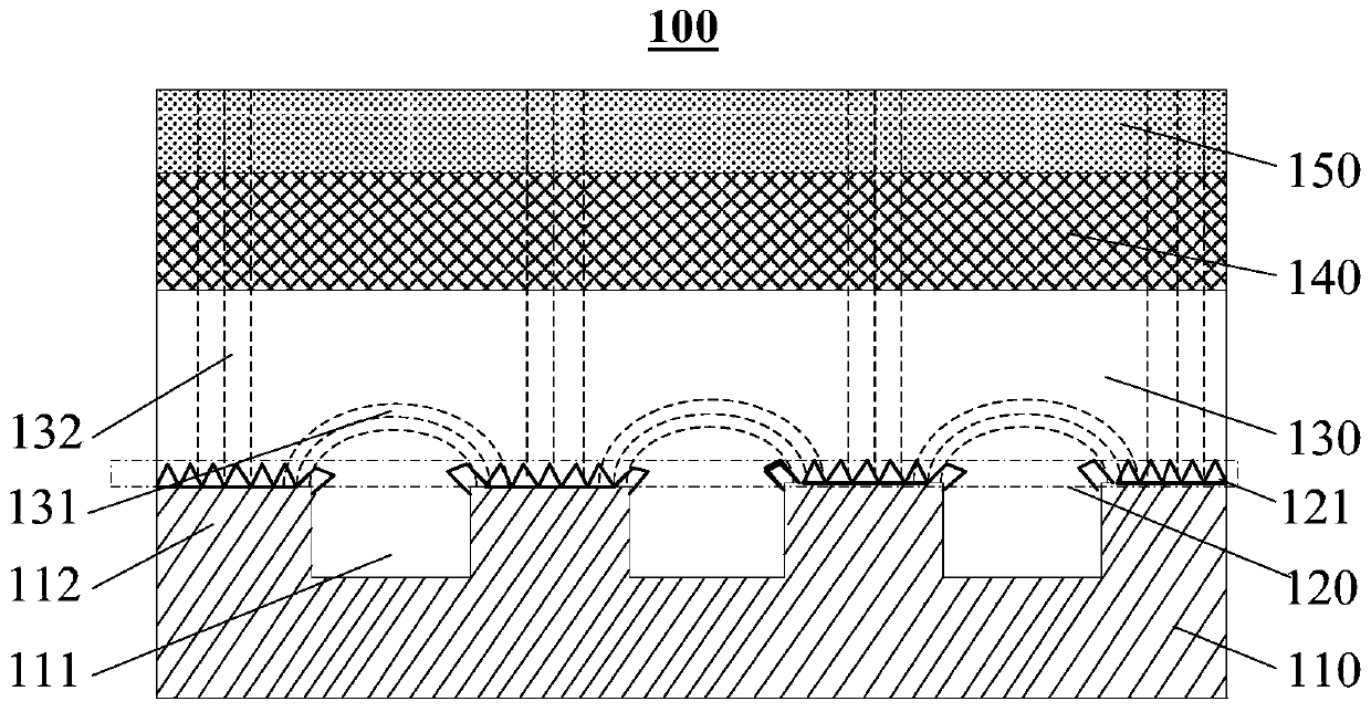
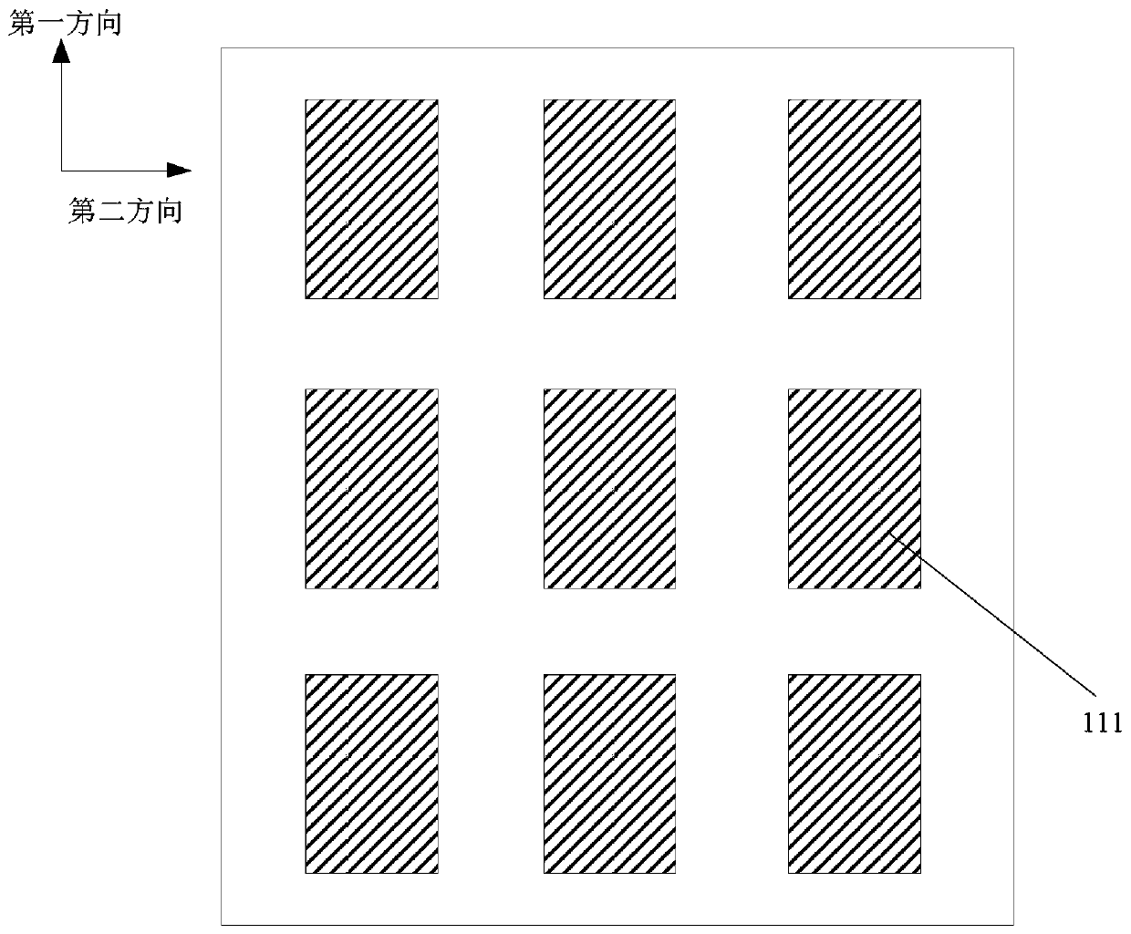
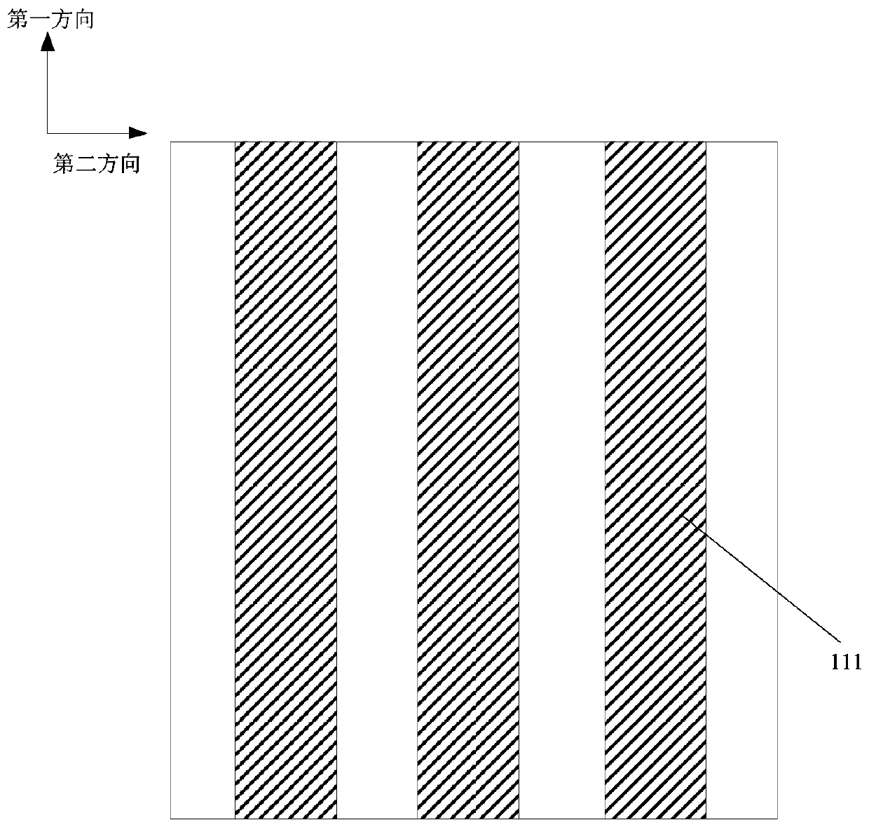
[0022] figure 1 A structural schematic diagram of an epitaxial structure of a III-nitride transistor provided by an embodiment of the present invention. Such as figure 1 As shown, the III-nitride transistor epitaxial structure 100 includes a substrate 110 and a nucleation layer 120, a buffer layer 130, a channel layer 140 and a barrier layer 150 stacked sequentially on the substrate; the substrate 110 includes multiple Each groove structure 111 and the growth window 112 between the groove structures 111; the nuc...


PUM


Abstract

The invention discloses an III-nitride transistor epitaxial structure comprising a substrate and a nucleation layer, a buffer layer, a channel layer and a barrier layer, which are sequentially stackedon the substrate, wherein the substrate comprises a plurality of groove structures and a growth window located among the groove structures; the nucleation layer is located in the growth window of thesubstrate; the buffer layer comprises a semi-polar III-nitride that is formed in a merging region and epitaxially grows along the direction of the growth window and the direction of the adjacent groove structure and a semi-polar III-nitride that is formed in the window region and epitaxially grows along the direction perpendicular to the plane where the substrate is located; the channel layer andthe barrier layer are both semi-polar III-nitrides, and the merged region and the window region both extend to the channel layer and the barrier layer. The III-nitride transistor epitaxial structurefacilitates the fabrication of enhanced HEMT devices with high electron mobility and low lateral leakage.

Description

technical field [0001] Embodiments of the present invention relate to the field of semiconductor materials and device manufacturing, and in particular to a III-nitride transistor epitaxial structure and a transistor device. Background technique [0002] Group III nitrides such as AlN, GaN, InN and their ternary and quaternary compounds are direct band gap compound semiconductor materials, which have wide band gap, high breakdown electric field and thermal conductivity, high electron mobility and chemical corrosion resistance, etc. Features, can fully meet the market demand for high-voltage conversion devices. [0003] At present, the GaN-based HEMT (High Electron Mobility Transistor, high electron mobility transistor) structure is mainly a c-plane polar material obtained by epitaxial growth on c-plane sapphire and (111)-plane Si substrates. It has strong spontaneous polarization and piezoelectric polarization along the growth direction, forming a large concentration of pola...

Claims


Application Information

Patent Timeline
Patent Type & Authority Applications(China)
IPC IPC(8): H01L29/10H01L21/335H01L29/778H01L29/06H01L29/20
CPCH01L29/66462H01L29/7787H01L29/1029H01L29/0688H01L29/2003
Inventor 何佳琦汪青于洪宇
Owner 珠海镓未来科技有限公司
Why Eureka
Try Eureka