Low-dark-current high-sensitivity photoelectric detector structure and manufacturing method thereof

A photodetector and high-sensitivity technology, applied in the direction of chemical instruments and methods, final product manufacturing, sustainable manufacturing/processing, etc., can solve the problems of production difficulty and cost increase, hinder side wall leakage, photocurrent influence, etc., to achieve Reduce the overlay and etching process, the process is simple, and the effect of improving device sensitivity

Pending Publication Date: 2021-11-12
全磊光电股份有限公司
View PDF0 Cites 0 Cited by
  • Summary
  • Abstract
  • Description
  • Claims
  • Application Information

AI Technical Summary

Problems solved by technology

[0005] Traditionally, there are two main ways to reduce the lateral dark current. One is the local isolation trench process, which forms a circle of isolation trenches around the detector absorption region through etching or oxidation processes to prevent sidewall leakage. In the increasingly shrinking integrated circuit technology, the requirements for the photolithographic overlay precision and etching precision of the chip technology are getting higher and higher, and the difficulty and cost of this isolation trench technology have increased significantly.
The other is the guard ring process commonly used in APD devices. In the annular space around the absorption region, the electric field is adjusted by implanting ions, thereby reducing the lateral leakage. This process also has the problems of complicated process and high cost, and in APD devices use, there is also an effect on the photocurrent

Method used


Image

  • Low-dark-current high-sensitivity photoelectric detector structure and manufacturing method thereof
  • Low-dark-current high-sensitivity photoelectric detector structure and manufacturing method thereof
  • Low-dark-current high-sensitivity photoelectric detector structure and manufacturing method thereof

Examples


Embodiment

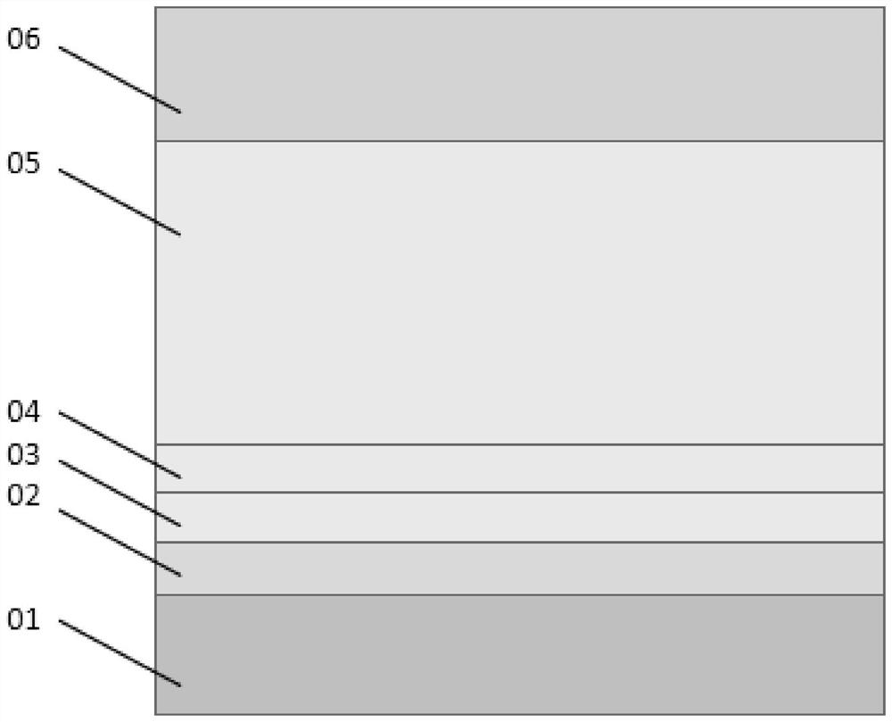
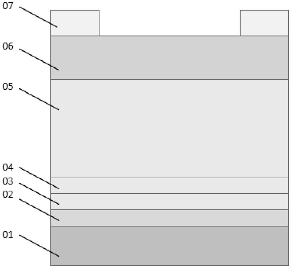
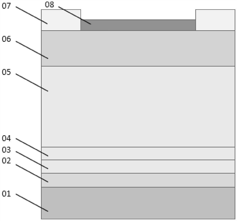
[0032] Example: such as image 3 As shown, a low dark current high-sensitivity photodetector structure includes an epitaxial wafer, the epitaxial wafer includes an InP substrate 01, and a buffer layer 02 and a lower ohmic contact layer 03 are sequentially deposited on the top of the InP substrate 01 from bottom to top. , transition layer 04, absorption layer 05 and window layer 06, upper ohmic contact layer 08 and insulating layer 08 are arranged above the window layer 06; upper ohmic contact layer 08 and insulating layer 07 are located in the same layer, insulating layer 07 is divided into two partly and respectively located on both sides of the upper ohmic contact layer 08 . The thickness of the insulating layer 07 is greater than the thickness of the upper ohmic contact layer 08 . Both parts of the insulating layer 07 have the same structure.

[0033] Its manufacturing method comprises the following steps:

[0034] Step 1: Use InP as the growth substrate, put it into the...


PUM


Abstract

A low-dark-current high-sensitivity photoelectric detector structure comprises an epitaxial wafer, the epitaxial wafer comprises an InP substrate, a buffer layer, a lower ohmic contact layer, a transition layer, an absorption layer and a window layer are sequentially deposited on the InP substrate from bottom to top, and an upper ohmic contact layer and an insulating layer are arranged on the window layer; and the upper ohmic contact layer and the insulating layer are located on the same layer, and the insulating layer is divided into two parts which are located on the two sides of the upper ohmic contact layer respectively. According to the invention, the detector epitaxial wafer with the isolation groove and the low side leakage structure is prepared by adopting the MOCVD selective area epitaxial process, the complex and high-precision photoetching overlay and etching process is reduced, the process is simplified, the yield is high, and the cost is low.

Description

technical field [0001] The invention belongs to the technical field of photodetector development, and in particular relates to a low dark current high-sensitivity photodetector structure and a manufacturing method thereof. Background technique [0002] Photodetectors are the key light-receiving devices in optical communication systems, and are widely used in optical communication systems, imaging systems and military fields, and are the commanding heights of science and technology seized by various countries. Photodetectors can generally be divided into two types: photodiode (PD) and avalanche photodiode (APD). Regardless of the type of photodetector, dark current is a key parameter of the core foundation. [0003] The dark current of photodetectors can be divided according to the relationship with the device size: the line dark current related to the circumference, the surface dark current related to the area, and the dark current compensation independent of the size. The ...

Claims


Application Information

Patent Timeline
Patent Type & Authority Applications(China)
IPC IPC(8): H01L31/18C30B25/18C30B25/20C30B28/14C30B29/40
CPCH01L31/1844C30B25/20C30B25/18C30B28/14C30B29/40Y02P70/50
Inventor 陈阳华张双翔张永单智发方天足
Owner 全磊光电股份有限公司
Why Eureka
Try Eureka