Scanning drive circuit and display device including the same

a drive circuit and drive circuit technology, applied in static indicating devices, cathode-ray tube indicators, instruments, etc., can solve the problems of poor uniformity of luminances in display devices, inability to disperse threshold voltages to a certain extent, etc., to reduce layout area occupied, reduce circuit cost, the effect of easy chang

Inactive Publication Date: 2013-04-02
SONY CORP
View PDF44 Cites 13 Cited by
  • Summary
  • Abstract
  • Description
  • Claims
  • Application Information

AI Technical Summary

Benefits of technology

[0035]In order to operate the display device including the display element described above, it is necessary to provide circuits for supplying signals to the scanning lines, the initialization control lines, and the display control lines, respectively. The circuits for supplying these signals are preferably a circuit having an integrated configuration from a viewpoint of reduction of a layout area occupied by these circuits, reduction of the circuit cost, and the like. In addition, the circuits preferably have such a configuration that setting of widths of pulses supplied to the display control lines, respectively, can be readily changed without exerting an influence on the signals supplied to the scanning lines and the initialization control lines, respectively, from a viewpoint of improving moving image characteristics by increasing a rate of the non-display time period.

Problems solved by technology

When transistors are composed of TFTs, it may be impossible that threshold voltages thereof disperse to a certain extent.
When amounts of currents caused to flow through the light emitting portions ELP, respectively, disperse along with a dispersion of the threshold voltages of the drive transistors TRD, uniformity of the luminances in the display device becomes worse.

Method used


Image

  • Scanning drive circuit and display device including the same
  • Scanning drive circuit and display device including the same
  • Scanning drive circuit and display device including the same

Examples


embodiment 1

[0127]A scanning drive circuit of the present invention, and a display device including the same will now be described based on Embodiment 1 thereof. The display device of Embodiment 1 is a display device using a display element including a light emitting portion and a circuit for driving the light emitting portion.

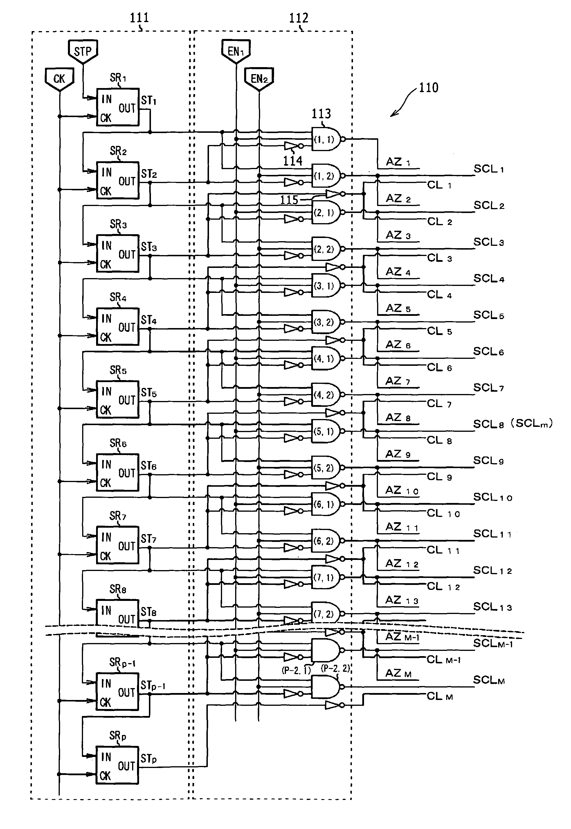
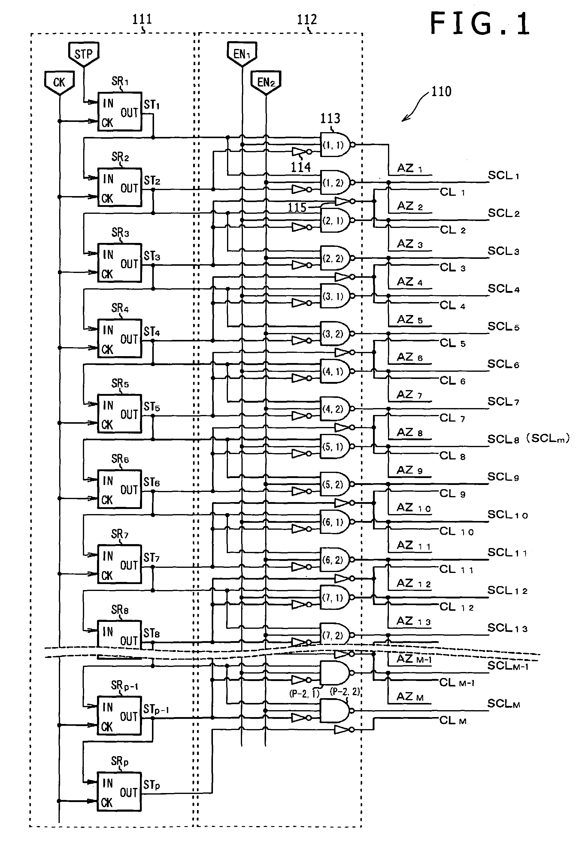
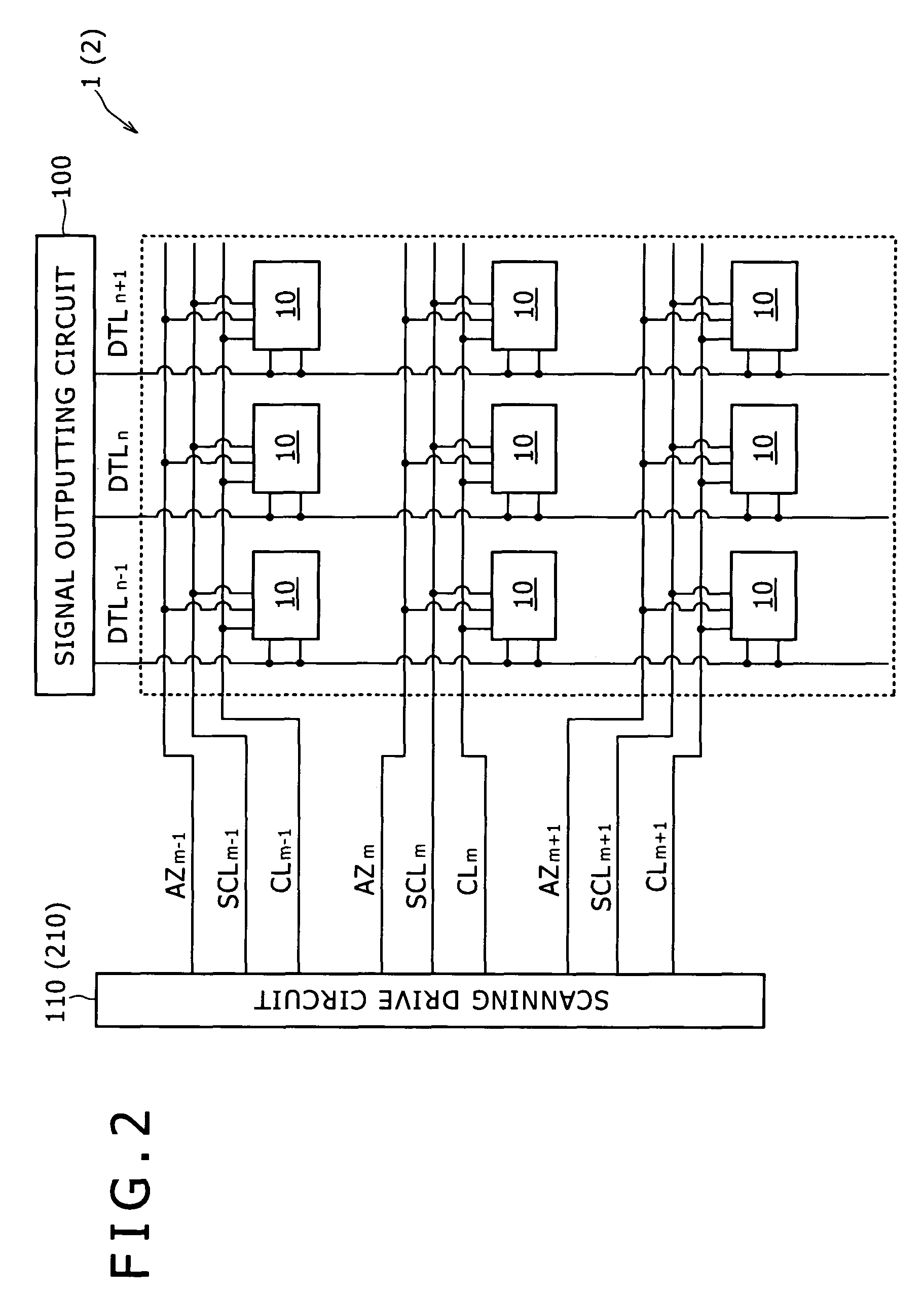
[0128]FIG. 1 is a circuit diagram showing a configuration of the scanning drive circuit 110 of Embodiment 1. FIG. 2 is a conceptual block diagram showing a configuration of the display device 1 of Embodiment 1 including the scanning drive circuit 110 shown in FIG. 1. FIG. 3 is a schematic timing chart explaining an operation of the scanning drive circuit 110 shown in FIG. 1. Also, FIG. 4 is an equivalent circuit diagram of a drive circuit 11 composing a display element 10 belonging to an m-th row (m=1, 2, 3, . . . , M) and an n-th column (n=1, 2, 3, . . . , N) in the display device 1 shown in FIG. 2. Firstly, an outline of the display device 1 will be described.

[0129]As s...

embodiment 2

[0222]A scanning drive circuit and a display device including the same according to the present invention will be described in detail hereinafter based on Embodiment 2. As shown in FIG. 2, the display device 2 of Embodiment 2 has the same configuration as that of the display device 1 of Embodiment 1 except that a scanning drive circuit 210 of the display device 2 of Embodiment 2 is different in configuration from the scanning drive circuit 110 of the display device 1 of Embodiment 1. Therefore, a description of the display device 2 is omitted in Embodiment 2 for the sake of simplicity.

[0223]FIG. 13 is a circuit diagram showing a configuration of the scanning drive circuit 210 of Embodiment 2. Also, FIG. 14 is a schematic timing chart explaining an operation of the scanning drive circuit 210 of Embodiment 2 shown in FIG. 13.

[0224]The scanning drive circuit 110 of Embodiment 1 uses the first enable signal EN1, and the second enable signal EN2. On the other hand, the scanning drive cir...


PUM


Abstract

A scan driving circuit and a display device, the display device including display elements two-dimensionally disposed in a matrix; scanning lines, initialization control lines, and display control lines extending in a first direction; and data lines extending in a second direction different from the first direction. The scan driving circuit includes a shift register portion and a logic circuit portion, and generates scan signals and initialization signals, both based on two or more enable signals, and control signals. The scan driving circuit is configured such that changing the width of a start pulse (and thereby the ratio of a light emitting period to a non-light emitting period) does not affect the scan signals or the initialization signals.

Description

BACKGROUND OF THE INVENTION[0001]1. Field of the Invention[0002]The present invention relates to a scanning drive circuit and a display device including the same. More particularly, the invention relates to a scanning drive circuit in which a ratio between a display time period and a non-display time period in each of display elements composing a display device can be readily adjusted, and a display device including the same.[0003]2. Description of the Related Art[0004]In addition to a liquid crystal display device composed of voltage-driven liquid crystal cells, a display device including a light emitting portion (for example, an organic electro-luminescence light emitting portion) which emits a light by causing a current to flow through the light emitting portion, and a drive circuit for driving the same are known as a display device including display elements two-dimensionally disposed in a matrix.[0005]A luminance of a display element including a light emitting portion which emi...

Claims


Application Information

Patent Timeline
Patent Type & Authority Patents(United States)
IPC IPC(8): G09G3/36
CPCG09G3/3266G09G5/001G09G2300/0861G09G2300/0819G09G3/20G09G3/30G09G3/3233G09G2310/0286G09G2310/08H05B47/10G09G3/32G09G3/3208G09G3/325G09G2300/0426G09G2300/0439
Inventor TANIKAME, TAKAOJINTA, SEIICHIRO
Owner SONY CORP
Why Eureka
Try Eureka