
Semiconductor device having CMOS transfer circuit and clamp element

a technology of transfer circuit and clamp element, which is applied in the direction of pulse generator, pulse technique, instruments, etc., can solve the problems of increasing the number of test pins in the test device, destroying the device or worsening the characteristics of the device, and the power supply voltage circuit of the semiconductor device has become complex, so as to accurately perform the measurement of the internal power supply voltage and accurately measure the potential of the internal power supply

Inactive Publication Date: 2013-04-16
RENESAS ELECTRONICS CORP
View PDF11 Cites 0 Cited by
  • Summary
  • Abstract
  • Description
  • Claims
  • Application Information

AI Technical Summary

Benefits of technology

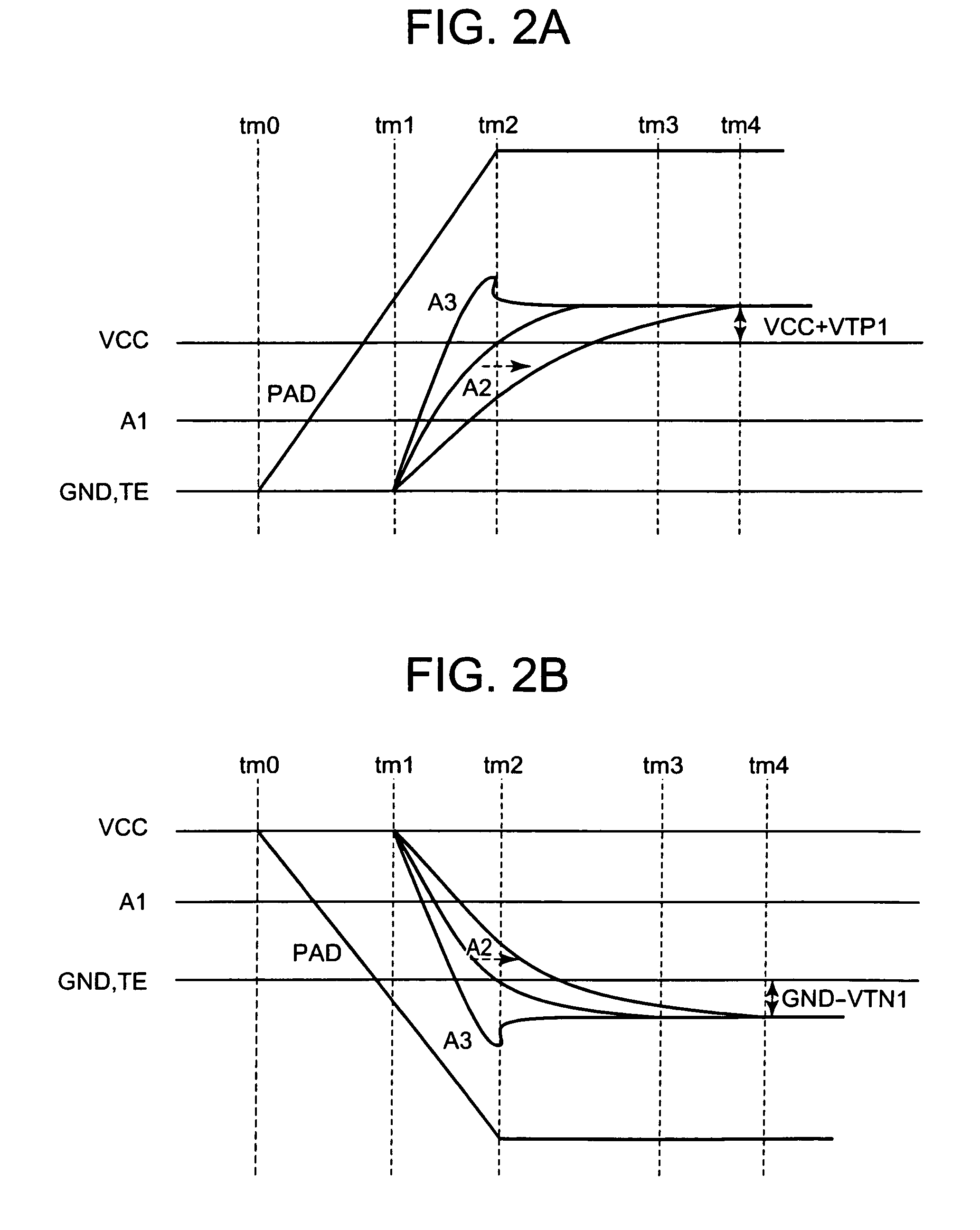
[0021]The first CMOS transfer circuit and the second CMOS transfer circuit are provided between the internal power-supply circuit and the external terminal, whereby it is possible to accurately measure the potential of an internal power supply even during low-voltage operations. The clamp circuit is provided between the first and second CMOS transfer circuits and a delay element is provided between the clamp element and the first CMOS transfer circuit, whereby it is possible to realize a measurement circuit of an internal power supply which is not affected by overshoots and undershoots from the external terminal.
[0022]According to the exemplary aspect, it is possible to provide a semiconductor device capable of accurately performing the measurement of the internal power-supply voltage of the semiconductor device even in low-voltage operations by providing the resistance against overshoots and undershoots.

Problems solved by technology

In recent years, the power-supply voltage circuit of a semiconductor device has become complex and a plurality of internal power-supply voltages, such as a step-down voltage, a step-up voltage, a negative voltage, and a half VCC, which is ½ of a power-supply voltage, are used in one chip.
When different voltages are generated within a device, this destroys the device or worsens the characteristics of the device.
However, because the number of test pins in a test device is insufficient, there has been increasing need for a measurement circuit of internal power-supply voltage which can be shared with external pins and permits high-accuracy measurements at low voltages.
In the case where terminals are shared like this, it has become an important problem to take measures to ensure that even when overshoots of not less than a power-supply voltage or undershoots of not more than GND enter external pins, this does not affect the internal potential.
In the semiconductor device shown in FIG. 6, a threshold value (hereinafter referred to as “VT”) of a transistor constituting the transfer circuit has an effect and, therefore, this poses the problem that it is impossible to accurately output an internal potential to outside the chip.
As shown in the simulation result, in a conventional circuit configuration, due to the effect of the VT of the transfer circuit during low-voltage operation, the measurement range of the internal power-supply voltage becomes narrow and the expected measurement of the internal power-supply voltage of a storage device becomes impossible.

Method used


Image

  • Semiconductor device having CMOS transfer circuit and clamp element
  • Semiconductor device having CMOS transfer circuit and clamp element
  • Semiconductor device having CMOS transfer circuit and clamp element

Examples


exemplary embodiment 1

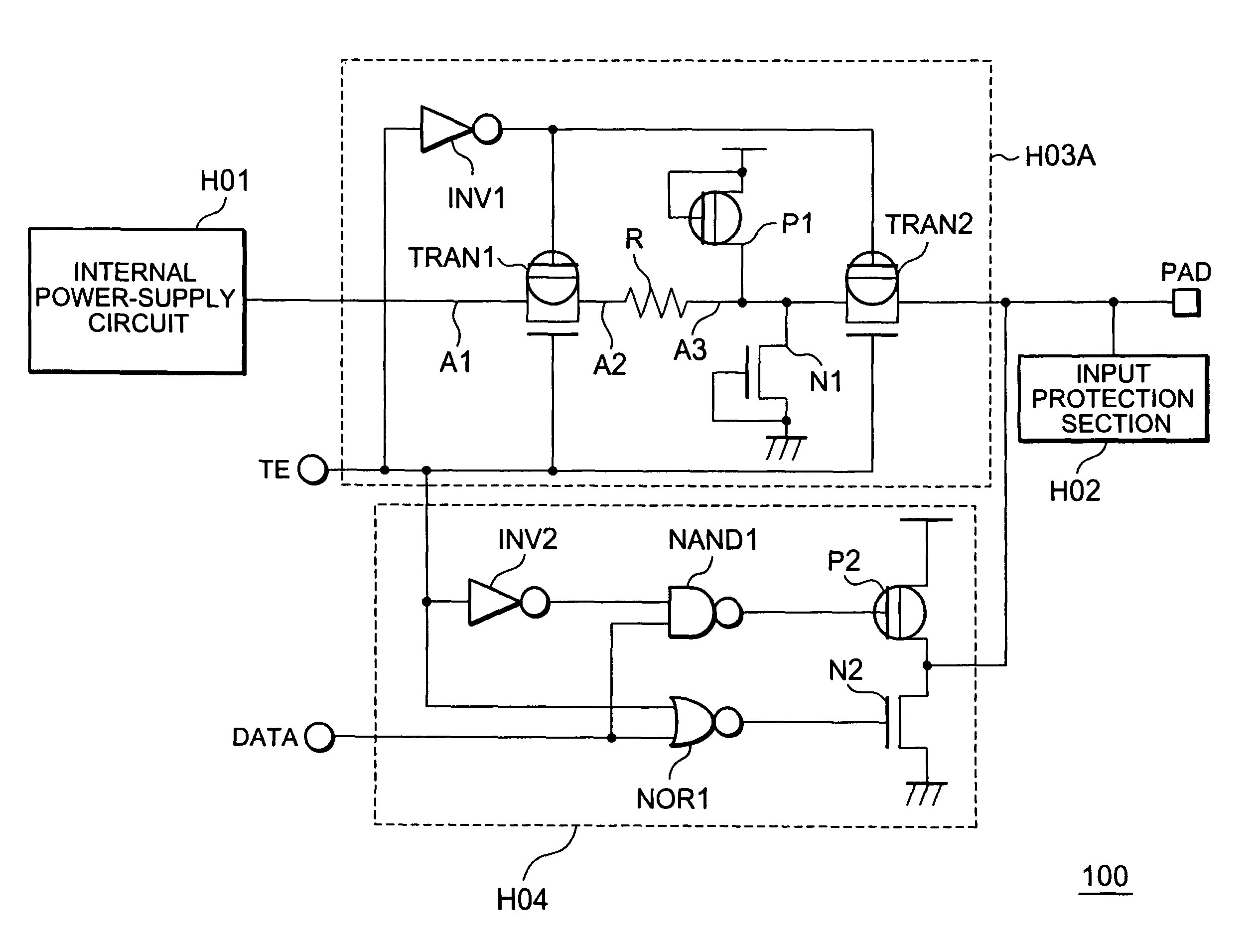
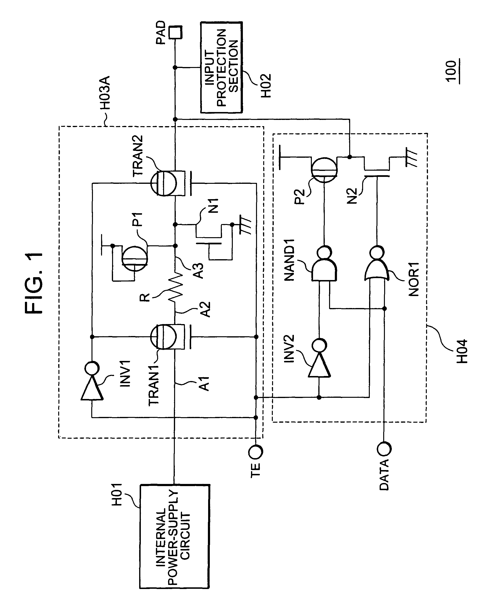
[0033]FIG. 1 is a circuit diagram showing the configuration of a semiconductor device 100 related to an exemplary embodiment of the present invention. As shown in FIG. 1, the semiconductor device 100 includes an internal power-supply circuit H01, an input protection section H02, a measurement circuit section H03A, an output circuit section H04, and an external terminal pad.

[0034]The semiconductor device 100 provides an example in which input and output pins and the external terminal pad which monitors the potential of the internal power-supply circuit H01 are shared. That is, the external terminal pad is a common-use external terminal which outputs the internal potential of the internal power-supply circuit H01 and performs the output and input of signals with the outside. An output of the output circuit section H04 is connected to the external terminal pad. The input protection section H02 is connected to a connection point between the output circuit section H04 and the external te...

exemplary embodiment 2

[0064]FIG. 3 is a circuit diagram showing the configuration of a semiconductor device 200 related to an exemplary embodiment 2. As shown in FIG. 2, the semiconductor device 200 includes an internal power-supply circuit H01, an input protection section H02, a measurement circuit section H03B, an output circuit section H04, and an external terminal pad. In this exemplary embodiment, what is different from the exemplary embodiment 1 is the configuration of a measurement circuit section H03B of internal power-supply voltage.

[0065]The measurement circuit section 03B solves the problem that the internal potential cannot be measured by using a CMOS transfer circuit. The measurement circuit section H03B blocks the effect of overshoots and undershoots from the external terminal pad on a measured point by using elements whose number is smaller than in the exemplary embodiment 1.

[0066]As shown in FIG. 3, in this exemplary embodiment, a clamp element NMOS transistor NM is provided in place of t...


PUM


Abstract

A semiconductor device includes an internal power-supply circuit which produces an internal potential, an external terminal which outputs the internal potential and inputs and outputs a signal with an outside, and a test mode signal terminal which transfers a test mode signal. The semiconductor device further includes a first CMOS transfer circuit and a second CMOS transfer circuit which are provided between the internal power-supply circuit and the external terminal, and which are controlled by the test mode signal, a clamp element which is connected between the first and second CMOS transfer circuits and suppresses a potential variation, and a delay element provided between the clamp element and the first CMOS transfer circuit.

Description

INCORPORATION BY REFERENCE[0001]This application is based upon and claims the benefit of priority from Japanese Patent Application No. 2009-022764 which was filed on Feb. 3, 2009, the disclosure of which is incorporated herein in its entirety by reference.BACKGROUND OF THE INVENTION[0002]1. Field of the Invention[0003]The present invention relates to a semiconductor device and, more particularly, to a semiconductor device provided with a measurement circuit of internal power-supply voltage.[0004]2. Description of Related Art[0005]In recent years, the power-supply voltage circuit of a semiconductor device has become complex and a plurality of internal power-supply voltages, such as a step-down voltage, a step-up voltage, a negative voltage, and a half VCC, which is ½ of a power-supply voltage, are used in one chip. Furthermore, because the breakdown voltage of a device has become lower due to miniaturization, the trend toward lower voltages has become more prevalent. When different v...

Claims


Application Information

Patent Timeline
Patent Type & Authority Patents(United States)
IPC IPC(8): G01R31/3187
CPCG01R19/0084G01R31/2884H03K3/356008
Inventor TASHIRO, SHINYATANIGUCHI, KAZUTAKA
Owner RENESAS ELECTRONICS CORP
Learn More