SiC power vertical DMOS with increased safe operating area

a vertical dmosfet and safe technology, applied in the direction of semiconductor devices, electrical apparatus, transistors, etc., can solve the problems of restricted soa of silicon power mosfets, non-uniformity, and inability to readily extend the method and structure of silicon power mosfet technology to make sic power mosfet devices

Active Publication Date: 2013-05-07
MICROSEMI
View PDF12 Cites 16 Cited by
  • Summary
  • Abstract
  • Description
  • Claims
  • Application Information

AI Technical Summary

Benefits of technology

[0019]It is an object of this invention to disclose methods and device structures suitable for a SiC Power MOSFET with increased SOA.
[0020]The foregoing and other objects, features and advantage

Problems solved by technology

However, the methods and structures employed in silicon power MOSFET technology do not readily extend to making SiC power MOSFET devices.
269-272) have shown that the SOA of silicon Power MOSFETs is in fact restricted on the high voltage high current side by the thermal instability of the device, with thermal instability triggered by the negative temperature coefficient of the Vth, if the device is operated at a drai

Method used


Image

  • SiC power vertical DMOS with increased safe operating area
  • SiC power vertical DMOS with increased safe operating area
  • SiC power vertical DMOS with increased safe operating area

Examples


Embodiment Construction

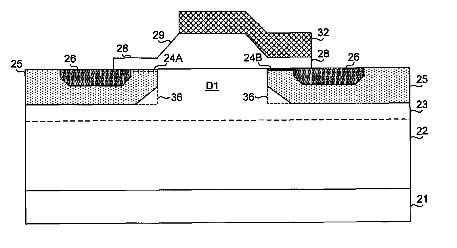
[0048]In the drawings, which are not necessarily to scale, like or corresponding elements of the SiC MOSFETs are denoted by the same referenced numerals.

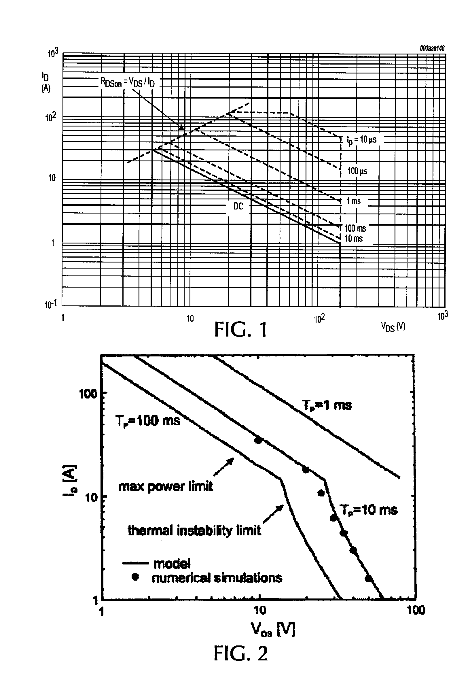
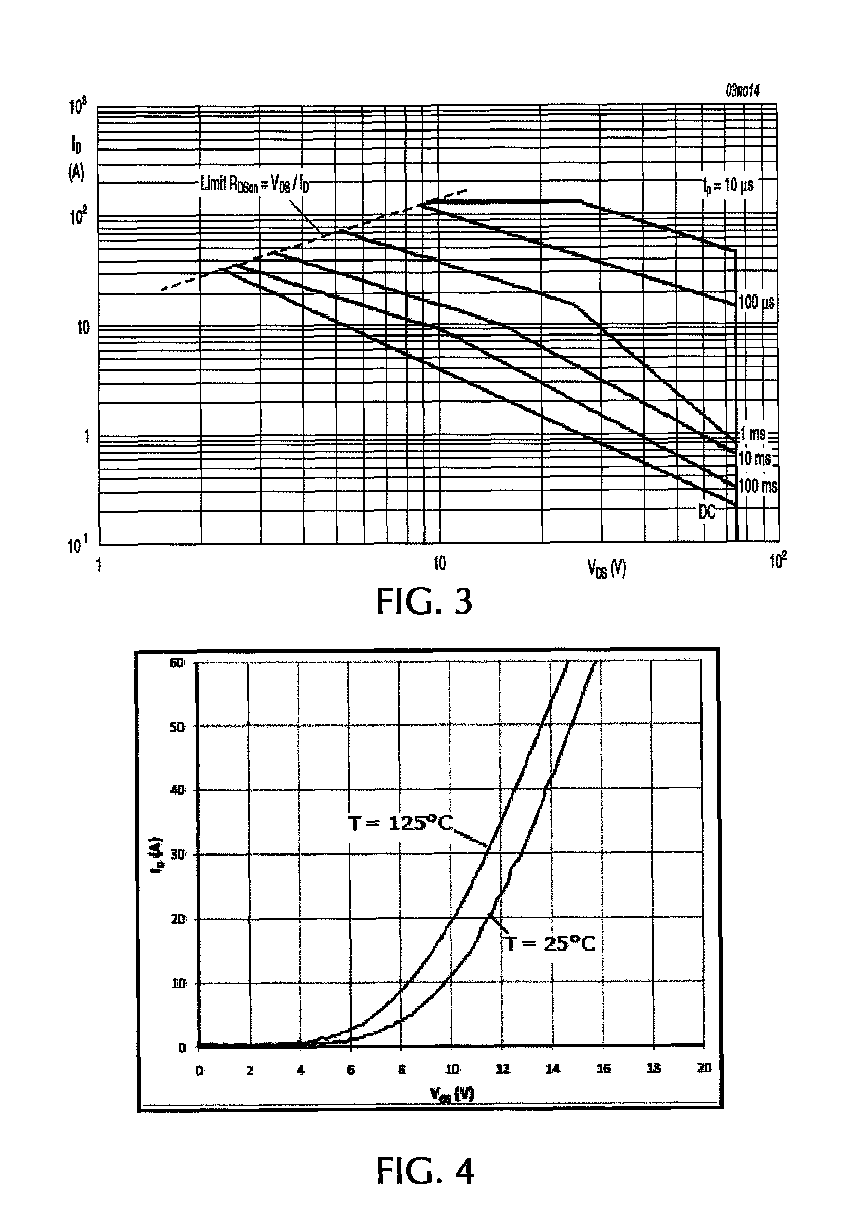
[0049]FIG. 1 represents an ideal SOA of a Power MOSFET made on Silicon or SiC. In reality, the power dissipation capability of the device is restricted at increased drain biases, as very well described in FIG. 2 and FIG. 3. An object of this invention is to “restore” the SOA of the Power MOSFET to its full capability across the entire voltage range.

[0050]The following will be clear for people skilled in the art and as explained in many publications on this topic of SOA of a Power MOSFET (for example see “Power Semiconductor Devices, Theory and Applications, Benda, Gowar, and Grant, John Wiley & Sons 1999). There are two mechanisms contributing to the destruction of the device while stressed under increased current and voltage conditions:[0051]the negative temperature coefficient of the drain / collector current in relationship to the ...


PUM


Abstract

A SiC Power Semiconductor device of the Field Effect Type (MOSFET, IGBT or the like) with “muted” channel conduction, negative temperature coefficient of channel mobility, in situ “ballasted” source resistors and optimized thermal management of the cells for increased Safe Operating Area is described. Controlling the location of the Zero Temperature Crossover Point (ZTCP) in relationship to the drain current is achieved by the partition between the “active” and “inactive” channels and by adjusting the mobility of the carriers in the channel for the temperature range of interest. The “Thermal management” is realized by surrounding the “active” cells/fingers with “inactive” ones and the “negative” feedback of the drain/collector current due to local increase of the gate bias is achieved by implementing in-situ “ballast” resistors inside of each source contact.

Description

CROSS REFERENCE TO RELATED APPLICATIONS[0001]This application claims the benefit of U.S. provisional patent application Ser. No. 61 / 382,087, filed Sep. 13, 2010, and is a continuation-in-part of copending U.S. application Ser. No. 13 / 195,632, filed Aug. 1, 2011, titled “Low Loss SiC MOSFET,” which claims the benefit of U.S. provisional patent application 61 / 369,765, filed Aug. 2, 2010, all herein incorporated by reference.FIELD OF THE INVENTION[0002]This invention pertains to Power MOSFET Semiconductor Devices to be used under such electrical conditions that the entire Safe Operating Area (hereinafter “SOA”) defined by the maximum allowed current and the maximum blocking voltage has to be available when the device is in the ON state, and more particularly to improving the SOA characteristics of silicon-carbide (SiC) vertical power MOSFET devices.BACKGROUND OF THE INVENTION[0003]Commonly-owned U.S. Pat. Nos. 6,503,786 and 6,664,594 to Klodzinski, incorporated herein by this reference...

Claims


Application Information

Patent Timeline
IPC IPC(8): H01L31/0312
CPCH01L29/42368H01L29/4238H01L29/456H01L29/66068H01L29/7802H01L29/0696H01L29/086H01L29/1033H01L29/105H01L29/1095H01L29/0865H01L29/0878H01L29/1608
Inventor SDRULLA, DUMITRUODEKIRK, BRUCEVANDENBERG, MARC
Owner MICROSEMI
Why Eureka
Try Eureka