Thin film photoelectric conversion device and method for manufacturing thin film photoelectric conversion device

a technology of conversion device and thin film, which is applied in the direction of semiconductor device, solid-state device, radiation control device, etc., to achieve the effect of high-sensitivity photo-induced current, excellent sensitivity characteristic, and small light loss

Inactive Publication Date: 2013-05-07
NUSOLA
View PDF21 Cites 0 Cited by
  • Summary
  • Abstract
  • Description
  • Claims
  • Application Information

AI Technical Summary

Benefits of technology

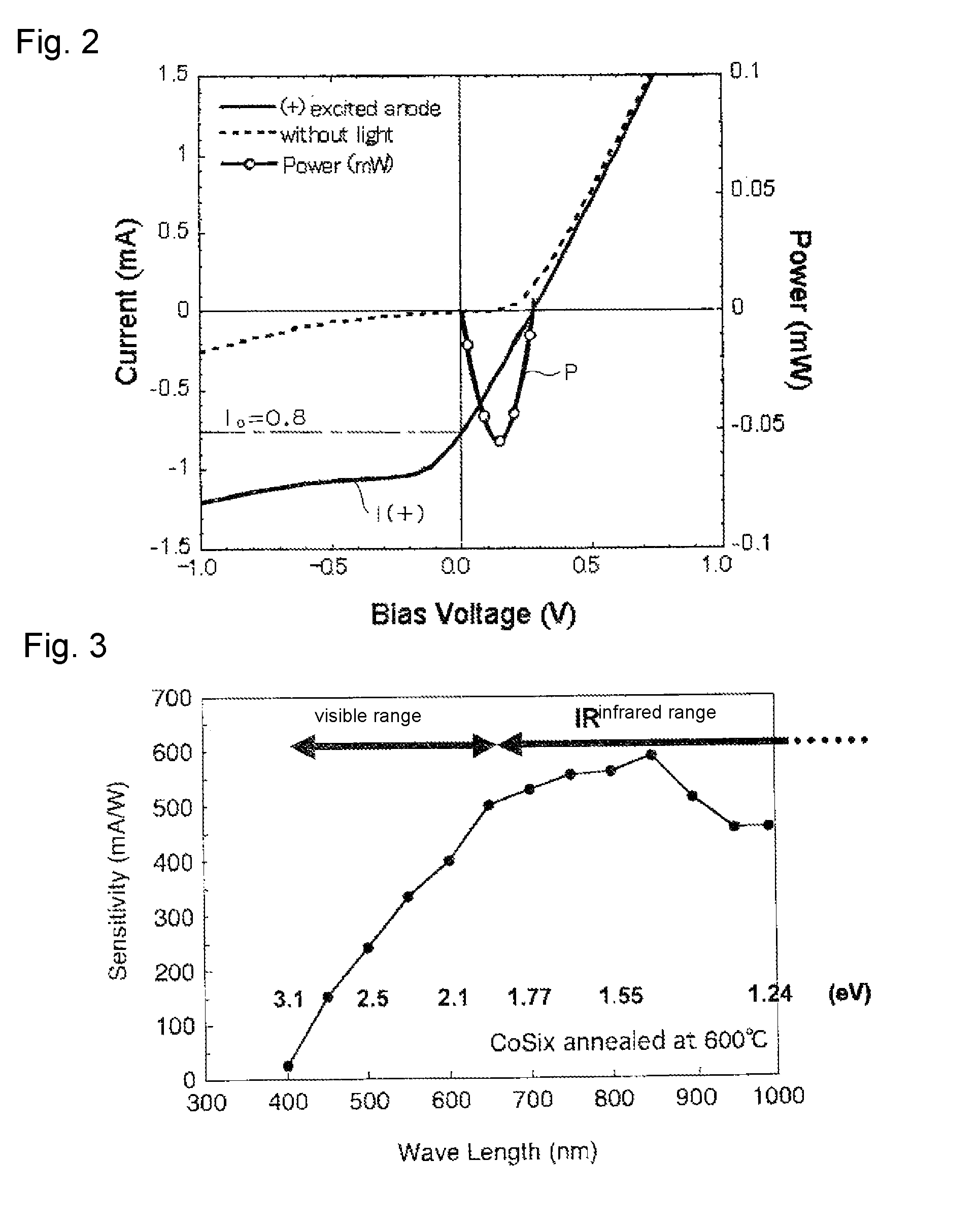
[0035]According to the invention of claim 1 and claim 7, photoelectric conversion of light having wide wavelength bands, from the visible range to the infrared range, can be performed in a manner independent on band gaps of materials of the substrate, such as silicon, at ordinary temperature without using harmful substances. Therefore, in the case where the thin film photoelectric conversion device is used as a light detecting sensor, its excellent sensitivity characteristic makes it possible to detect a wide range of light. Further, in the case where the thin film photoelectric conversion device is used as a solar cell, it is possible to perform photoelectric conversion of a wide range of sunlight to utilize it as electric power, and in particular when the sky is cloudy, it is possible to utilize, as electric power, about twice more solar energy than that utilized in the case of solar cells using p-n junction Si-based photoelectric conversion devices. Furthermore, by performing photoelectric conversion of infrared light scattered from the atmosphere after sunset, day / night power generation is expected. As the photoelectric conversion of the scattered infrared light is performed before the scattered infrared light is converted into heat, this is expected as a measure against global warning, as well.
[0036]The present invention is not for performing photoelectric conversion of light which transmits inside the substrate, but for performing photoelectric conversion at the surface of the substrate, and therefore, light loss is small and high sensitivity photo-induced current can be obtained.
[0037]Further, as photocarriers diffuse along the surface of the substrate, high speed photo-induced carriers with diffusion speed of about 107 cm / s, which is comparable to the speed of compound semiconductors, are generated. Therefore, when used as a light detecting sensor, it is possible to realize a photoelectric conversion device which responds to an ultra-high speed image sensor, or to optical modulation waves in the GHz to THz band. As it is thin-film type, it is possible to use it as a surface-detecting CCD sensor which can be arrayed.
[0038]In addition, because majority carriers are generated at the interface of the barrier along the surface of the semiconductor substrate and the storage effect of minority carriers can be negligible, it becomes possible to reduce noise in comparison to pn junction optical sensors, and when it is used for solar cells, coexistence of p-type and n-type carriers is suppressed and there is no decrease in the conversion efficiency caused by recombination of them.
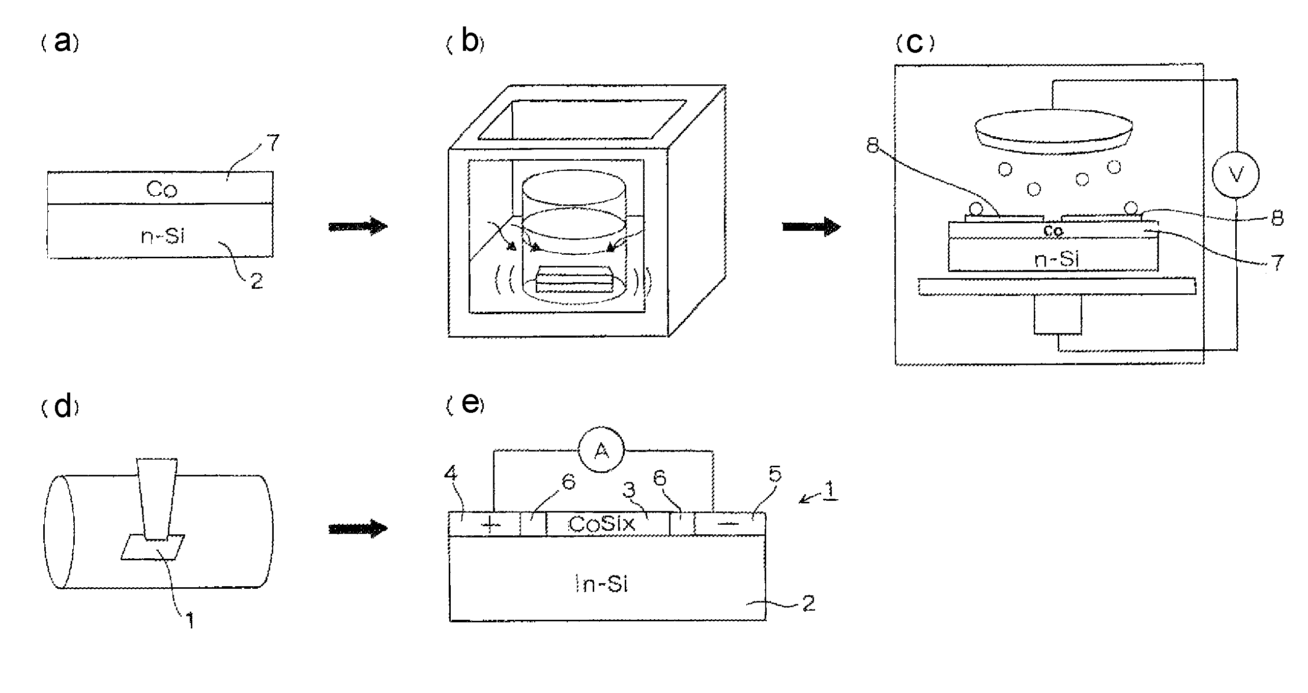
[0039]According to the invention of claim 7, in particular, the thin film photoelectric conversion device can be manufactured by a simple manufacturing process, only laminating the first metal thin film layer and the second metal thin film layer on the substrate and annealing the substrate, and it can be manufactured by just using very small amount of scarce elements in the manufacturing process.
[0040]According to the invention of claim 2, the periodic structure and the random structure, whose structures are different from each other, can be present in a mixed state in the same planar region by making differentiation between the heights of the second convex part and the first convex part from the substrate.
[0041]According to the invention of claim 3 and claim 8, generation of the photocarriers, high-efficiency generation of photocarriers caused by the enhancement of the photo-induced electric field and output of the photo-induced current by the generated photocarriers can be realized only on the surface of one device.
[0042]In addition, as the photo-induced current can be generated by only using the conductive thin film layer and the metal nanostructure on the surface of the substrate, the thickness can be reduced. When the thin film photoelectric conversion device is used for solar cells, it is possible to attach it to windows of buildings or automobiles, or housings for portable equipment such as mobile phones, and no restriction is applied to location to be attached.
[0043]Further, according to the invention of claim 4 and claim 8, the first electrode ohmic connected to the conductive thin film layer and the metal nanostructure can be formed by the process for forming the conductive thin film layer.
[0044]According to the invention of claim 5 and claim 9, the Si-based process for forming a metal silicide can be used. In addition, the metal silicide which forms the conductive thin film layer suppresses excessive diffusion of the second metal, which is an electrode-forming material, into the silicon substrate, and can prevent oxidation of silicon.
[0045]According to the invention of claim 6 and claim 10, the first metal and the second metal which is a noble metal can be manufactured from very small amount of scarce elements because both of them are used only for forming the metal thin film layers.
[0046]The first metal has a high melting point, is excellent in mechanical property at high temperature, and suitable as a material for the metal silicide. In particular, in the case where the first metal is Co, the metal silicide is CoSix used for an electrode underlayer of a silicon device, and an existing process can be used. Further, the second metal is chemically stable, hard to combine with silicon, and easy to form a metal nanostructure.

Problems solved by technology

Further, many of the photoelectric conversion devices used for solar cells are pn-junction-type photoelectric conversion devices formed on Si substrates, and their availability for use is limited to sunlight having wavelengths equal to or shorter than 1.2 μm due to the band gap of Si, and therefore, they are mainly used for performing photoelectric conversion of visible light having wavelengths equal to or shorter than 0.8 μm.

Method used


Image

  • Thin film photoelectric conversion device and method for manufacturing thin film photoelectric conversion device
  • Thin film photoelectric conversion device and method for manufacturing thin film photoelectric conversion device
  • Thin film photoelectric conversion device and method for manufacturing thin film photoelectric conversion device

Examples


example 1

[0097]A Co thin film with a thickness of 8 nm was formed by sputtering on the entire surface of an n-Si substrate composed of n-type Si having a roughly square shape, and organic cleaning was performed for 5 minutes, then mask printing was performed and a Au thin film with a thickness of about 10 nm was formed on four corners and center of the surface of the square Co thin film by sputtering. Subsequently, annealing was performed under the condition of heating-up time of 1 minute, annealing temperature of 600° C., annealing time of 3 minutes to obtain the thin film photoelectric conversion device 30 in which each of the following components was formed: a CoSix layer 31 with a thickness equal to or smaller than 10 nm, which is a conductive thin film layer self-assembled on the surface of the n-Si substrate; a cathode electrode ohmic connected to the CoSix layer 31 on the four corners of the substrate; an anode electrode 41 ohmic connected to the CoSix layer 31 in the center of the su...


PUM

PropertyMeasurementUnit
distanceaaaaaaaaaa
wavelengthsaaaaaaaaaa

Abstract

A thin film photoelectric conversion device for performing photoelectric conversion of a wide range of light, from the visible range to the infrared range, is provided. A plasmon resonance phenomenon, which enhances a photo-induced electric field, is caused in a wide range of light, by a metal nanostructure which is formed by annealing a substrate on which a first metal thin film layer composed of a first metal and a second metal thin film layer composed of a second metal which is partially overlapped onto the first metal thin film layer are laminated, and in which a periodic structure, wherein a number of first convex parts successively lie with a pitch of from one-tenth of a wavelength of an incident light to a wavelength equal to or shorter than the wavelength of the incident light in a planar direction along the substrate, is formed on the surface of the substrate; and a random structure, wherein a distance between any pair of a number of second convex parts formed at random positions on the substrate, or a distance between a second convex part and a first convex part is shorter than 100 nm, is formed on the substrate in a position within a region of the periodic structure or in a position adjacent to the region of the periodic structure, and as a result, high sensitivity photo-induced current is generated.

Description

TECHNICAL FIELD[0001]The present invention relates to a thin film photoelectric conversion device and a method for manufacturing the thin film photoelectric conversion device, and more particularly, to a thin film photoelectric conversion device which causes generation of photocarriers on a surface of the device and a method for manufacturing the thin film photoelectric conversion device.BACKGROUND ART[0002]Many of the photoelectric conversion devices used for optical sensors or solar cells use semiconductor crystals such as Si and GaAs, and require precise doping control, control of a pn junction interface or a Schottky interface, and microstructure fabrication techniques.[0003]Further, many of the photoelectric conversion devices used for solar cells are pn-junction-type photoelectric conversion devices formed on Si substrates, and their availability for use is limited to sunlight having wavelengths equal to or shorter than 1.2 μm due to the band gap of Si, and therefore, they are...

Claims


Application Information

Patent Timeline
Patent Type & Authority Patents(United States)
IPC IPC(8): H01L31/18H01L31/04H01L31/09
CPCH01L31/0352H01L31/04H01L31/09Y02E10/50H01L31/18
Inventor BRICENO, JOSE
Owner NUSOLA
Why Eureka
Try Eureka