
Anodic bonding method and piezoelectric vibrator manufacturing method

a piezoelectric vibrator and manufacturing method technology, applied in the direction of electrical equipment, chemistry apparatus and processes, lamination ancillary operations, etc., can solve the problems of air trapped, voids formed in non-bonded areas, excessive voltage application, etc., to suppress the excess application of dc voltage at the central side of the concentric intended bonding area, improve the productivity of the piezoelectric vibrator, and suppress the uneven quality of the bonding surface

Inactive Publication Date: 2013-05-21
SEIKO INSTR INC
View PDF3 Cites 0 Cited by
  • Summary
  • Abstract
  • Description
  • Claims
  • Application Information

AI Technical Summary

Benefits of technology

[0013]The present invention has been made in view of the foregoing, and an object of the present invention is to provide an anodic bonding method capable of suppressing uneven quality between the central and outer sides of a bonding surface being anodically bonded. Another object of the present invention is to provide a piezoelectric vibrator manufacturing method capable of improving productivity of a piezoelectric vibrator by using the anodic bonding method in manufacturing the piezoelectric vibrator.
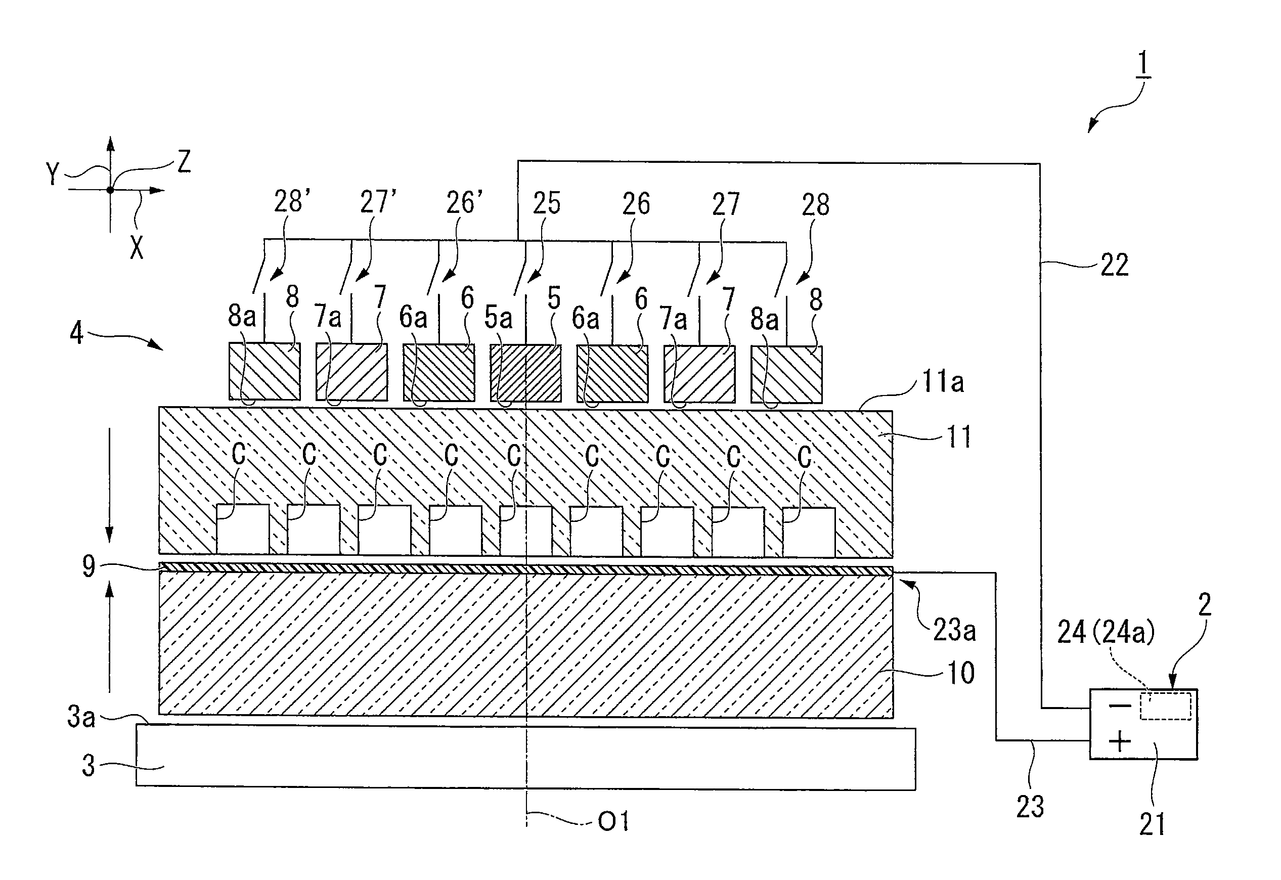
[0016]According to the above aspect of the present invention, the DC voltage applied to each area of the first glass substrate and the second glass substrate is the same in any of the concentric intended bonding areas. Therefore, excessive application of the DC voltage at the central side of the concentric intended bonding areas can be suppressed. Thus, it is possible to suppress uneven quality of the bonding surface which is the contacting surface after the anodic bonding.
[0019]In this case, it is possible to apply the DC voltage while sequentially switching the central electrode and the plurality of annular electrodes from the central side toward the outer side. Therefore, it is possible to easily switch the concentric intended bonding areas.
[0025]According to the above aspect of the present invention, the DC voltage applied to each area of the first glass substrate and the second glass substrate is the same in any of the concentric intended bonding areas. Therefore, excessive application of the DC voltage at the central side of the concentric intended bonding areas can be suppressed. Thus, it is possible to suppress uneven quality of the bonding surface which is the contacting surface after the anodic bonding and improve productivity of the piezoelectric vibrator.
[0026]According to the anodic bonding method according to the above aspect of the present invention, it is possible to suppress uneven quality between the central and outer sides of a bonding surface being anodically bonded. According to the piezoelectric vibrator manufacturing method according to the above aspect of the present invention, it is possible to improve productivity of a piezoelectric vibrator by using the anodic bonding method in manufacturing the piezoelectric vibrator.

Problems solved by technology

Thus, there is a problem in that air is trapped in areas between a plurality of bonding portions, which remain unbonded all the way on the bonding surfaces, and voids are formed in the non-bonded areas.
In this case, in the bonding portion at the central side of the insulating material, the voltage would be applied for an excessively long period even though it has been bonded completely.
Moreover, in the area where the voltage is applied for an excessively long period, much gas will be generated during the anodic bonding.
The gas generated at the interface of the metal and the insulating material after the anodic bonding will become the cause of defects of the anodic bonding like the voids.
Therefore, there is a problem in that the bonding surface between the metal and the insulating material anodically bonded by the anodic bonding method disclosed in JP-A-63-229853 exhibits uneven quality between the central and outer sides.
This problem will be more noticeable when large-size substrates are anodically bonded.
In addition, when piezoelectric vibrators, semiconductor components, and the like were manufactured by anodically bonding a metal wafer and an insulator wafer in accordance with the anodic bonding method disclosed in JP-A-63-229853, there is a concern that the bonding surface quality becomes uneven between the central and outer sides of the bonding surface of the wafer, thus causing bonding defects in the piezoelectric vibrators, semiconductor components, and the like.

Method used


Image

  • Anodic bonding method and piezoelectric vibrator manufacturing method
  • Anodic bonding method and piezoelectric vibrator manufacturing method
  • Anodic bonding method and piezoelectric vibrator manufacturing method

Examples


first modification

[0101]Another configuration of a base wafer applicable to the above-described anodic bonding method will be described.

[0102]FIG. 8 is a sectional view showing the configuration of a base wafer and a lid wafer which can be applied to the anodic bonding method according to the above-described embodiment.

[0103]As shown in FIG. 8, in this modification, a base wafer 10a is used in place of the base wafer 10. The base wafer 10a has second cavities C2 which are disposed at positions where they face the cavities C in a state where the base wafer 10a is superimposed onto the lid wafer 11 and which have an opening having the same shape and size as the opening of each of the cavities C of the lid wafer 11 so that the openings can be superimposed on the openings of the cavities C. When the base wafer 10a and the lid wafer 11 are superimposed in the superimposition step (step S31), the openings of the cavities C oppose the openings of the cavities C2, and the cavities C and C2 each form one isol...

second modification

[0105]A second modification of the above-described embodiment will be described.

[0106]FIG. 9 is a sectional view showing the configuration of a base substrate and a lid substrate which can be applied to the anodic bonding method according to the above-described embodiment. As shown in FIG. 9, in this modification, the anodic bonding machine 1 is provided with an anode electrode 30 having the function of an anode in place of the setting table 3. The anode electrode 30 has a setting surface 3a on which the base wafer 10 is set, similarly to the setting table 3, and which is made of a conductive material. In this modification, the bonding film 9 of the base wafer 10 is not used as the electrode of the anodic bonding.

[0107]In this modification, the positive terminal of the power supply 2 and the anode electrode 30 are connected by the anode-side wiring 23. In this way, positive ions of the lid wafer 11 are moved towards the cathode electrode 4 between the bonding film 9 and the lid wafe...

third modification

[0109]A third modification of the above-described embodiment will be described.

[0110]In this modification, the setting values of the lengths of the application times T1, T2, T3, and T4 in the above-described embodiment are different from the setting values.

[0111]First, as shown in FIG. 6, a DC voltage is applied to the central electrode 5 to form the bonding surface Q1 in the intended bonding area A1 which is the same as the above-described embodiment.

[0112]Subsequently, the intended bonding area A2 shown in FIG. 7A is anodically bonded by using the central electrode 5. In the related art, a method of bringing a needle-like electrode into contact with one point on a substrate to widen the bonding surface (for example, the bonding surface Q1) in a radial form (concentric form) from the one point is known. In this modification, it is possible to widen the bonding surface in the order of the bonding surfaces Q1 and Q2 by using the central electrode 5. That is, an application time T1′ d...


PUM

PropertyMeasurementUnit
temperatureaaaaaaaaaa
pressing forceaaaaaaaaaa

Abstract

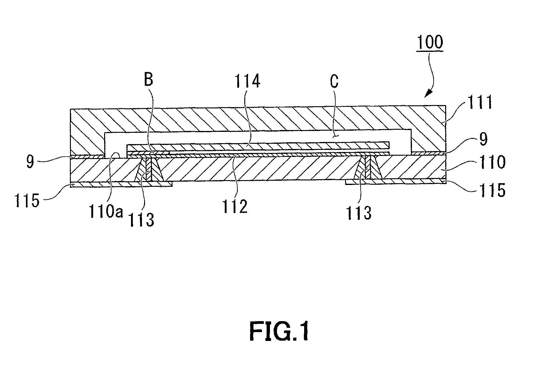
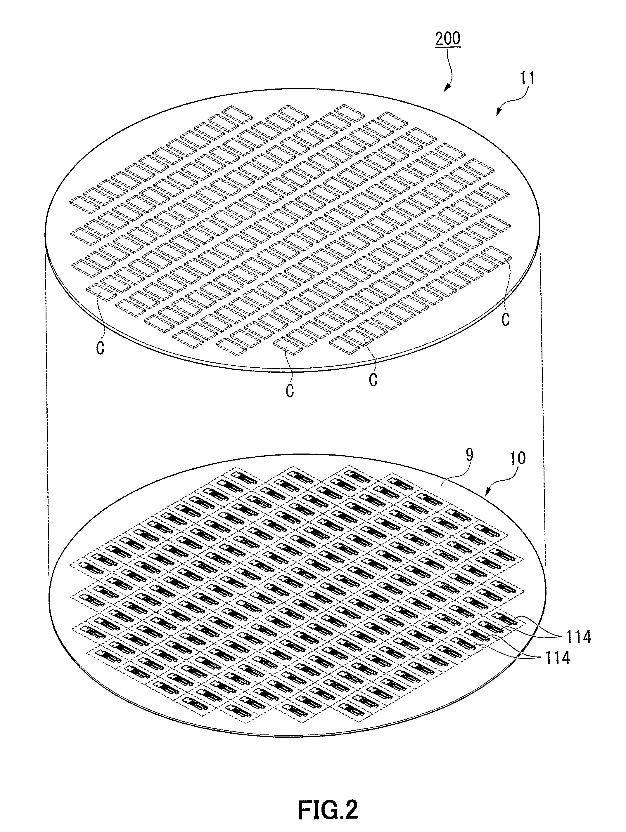
An anodic bonding method of anodically bonding a base wafer 10 and a lid wafer 11 includes:(1) superimposing the base wafer 10 and the lid wafer 11 onto each other in a direction where a bonding film 9 faces a cavity C; (2) subsequent to the superimposition step, pressurizing and holding the base wafer 10 and the lid wafer 11 in a vacuum state in the superimposition direction; and (3) subsequent to the pressurizing step, partitioning and setting a plurality of intended bonding areas A1, A2, A3 and A4 in a concentric form on a contacting surface where the base wafer 10 and the lid wafer 11 are in contact with each other and applying a DC voltage to each of the plurality of intended bonding areas A1, A2, A3 and A4.

Description

RELATED APPLICATIONS[0001]This application claims priority under 35 U.S.C. §119 to Japanese Patent Application No. 2009-195965 filed on Aug. 26, 2009, the entire content of which is hereby incorporated by reference.BACKGROUND OF THE INVENTION[0002]1. Field of the Invention[0003]The present invention relates to an anodic bonding method and a piezoelectric vibrator manufacturing method.[0004]2. Description of the Related Art[0005]In the related art, in the manufacturing process of piezoelectric vibrators or semiconductor components, anodic bonding has been performed to bond a silicon wafer or the like to the surface of an insulating material such as glass.[0006]The anodic bonding is a method of bringing metal, silicon, or the like to be bonded into contact with one surface of an insulating material such as glass and bringing a cathode made of metal into contact with the other surface of the insulating material, thus bonding the metal and the insulating material together with the appli...

Claims


Application Information

Patent Timeline
Patent Type & Authority Patents(United States)
IPC IPC(8): B29C65/14
CPCH03H3/02H03H9/1014
Inventor ARATAKE, KIYOSHI
Owner SEIKO INSTR INC
Learn More