Display device and flat display device

a display device and display device technology, applied in the field of display devices, can solve the problems of repeated exposure of the cof to deformation, and achieve the effects of enhancing the reliability of a flat display device, preventing the concentration of bending stress, and preventing the disconnection of lines

Active Publication Date: 2013-06-04
JAPAN DISPLAY INC
View PDF11 Cites 11 Cited by
  • Summary
  • Abstract
  • Description
  • Claims
  • Application Information

AI Technical Summary

Benefits of technology

[0030]By adopting the above-mentioned constitution, the present invention can enhance the reliability of the connection between the display panel and the external circuit. To explain advantageous effects obtained by the above-mentioned respective constitutions, they are as follows.
[0031]According to the constitution (1), even when the wiring film is bent, it is possible to prevent the concentration of bending stress on the branching portions of the lines and hence, it is possible to prevent the disconnection of the lines of the wiring film thus enhancing the reliability of a flat display device.
[0032]According to the constitution (2), when the terminal portion formed on the substrate of the display device is large, the plurality of lines of the wiring film can be connected and hence, the thermosetting condition in the connection process becomes uniform whereby the reliability of the connection portion can be enhanced. Further, even when such a constitution is adopted, due to the present invention, it is possible to prevent the disconnection or the like attributed to the bending stress applied to the wiring film.
[0033]According to the constitution (3), even when the line having the large width formed on the wiring film is branched into three or more lines having the narrow width, the branching positions can be changed and hence, the concentration of stress when the wiring film is bent can be further prevented.
[0034]According to the constitution (4), by arranging the dummy line between the lines which are formed on the wiring film and are connected with the substrate, the reliability of the connection portion can be increased and, at the same time, the dummy line performs a function of alleviating the concentration of bending stress.
[0035]According to the constitution (5), the wiring film is bent along the side portion of the display device and hence, the display device can be formed in a compact shape. At the same time, due to the above-mentioned constitution, even when bending stress is continuously applied to the wiring film, the concentration of the bending stress applied to the branching portions can be alleviated thus preventing the disconnection of the lines.

Problems solved by technology

Further, due to driving of the liquid crystal display panel or a change of an ambient temperature, the COF is repeatedly exposed to the deformation attributed to the difference in thermal expansion between a TFT substrate and a printed circuit board.

Method used


Image

  • Display device and flat display device
  • Display device and flat display device
  • Display device and flat display device

Examples


embodiment 1

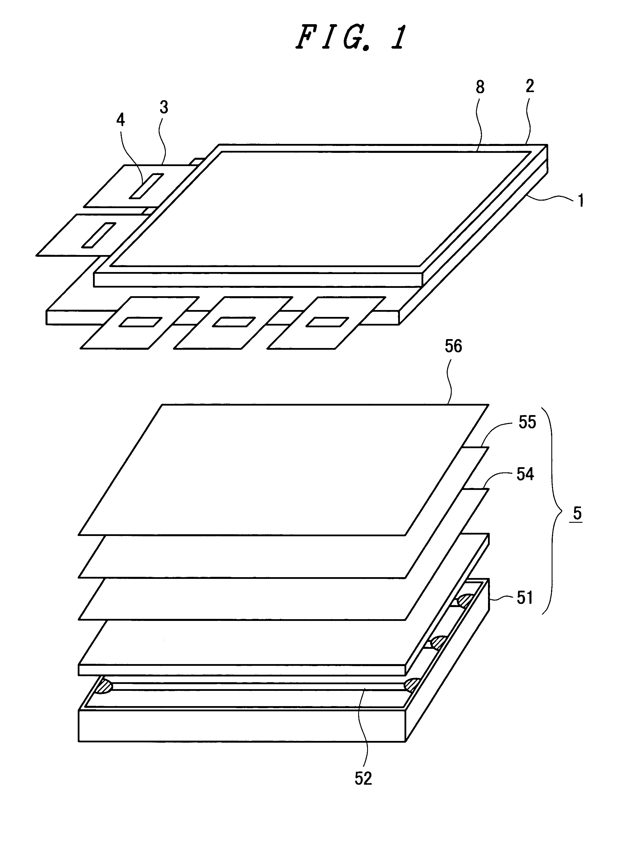
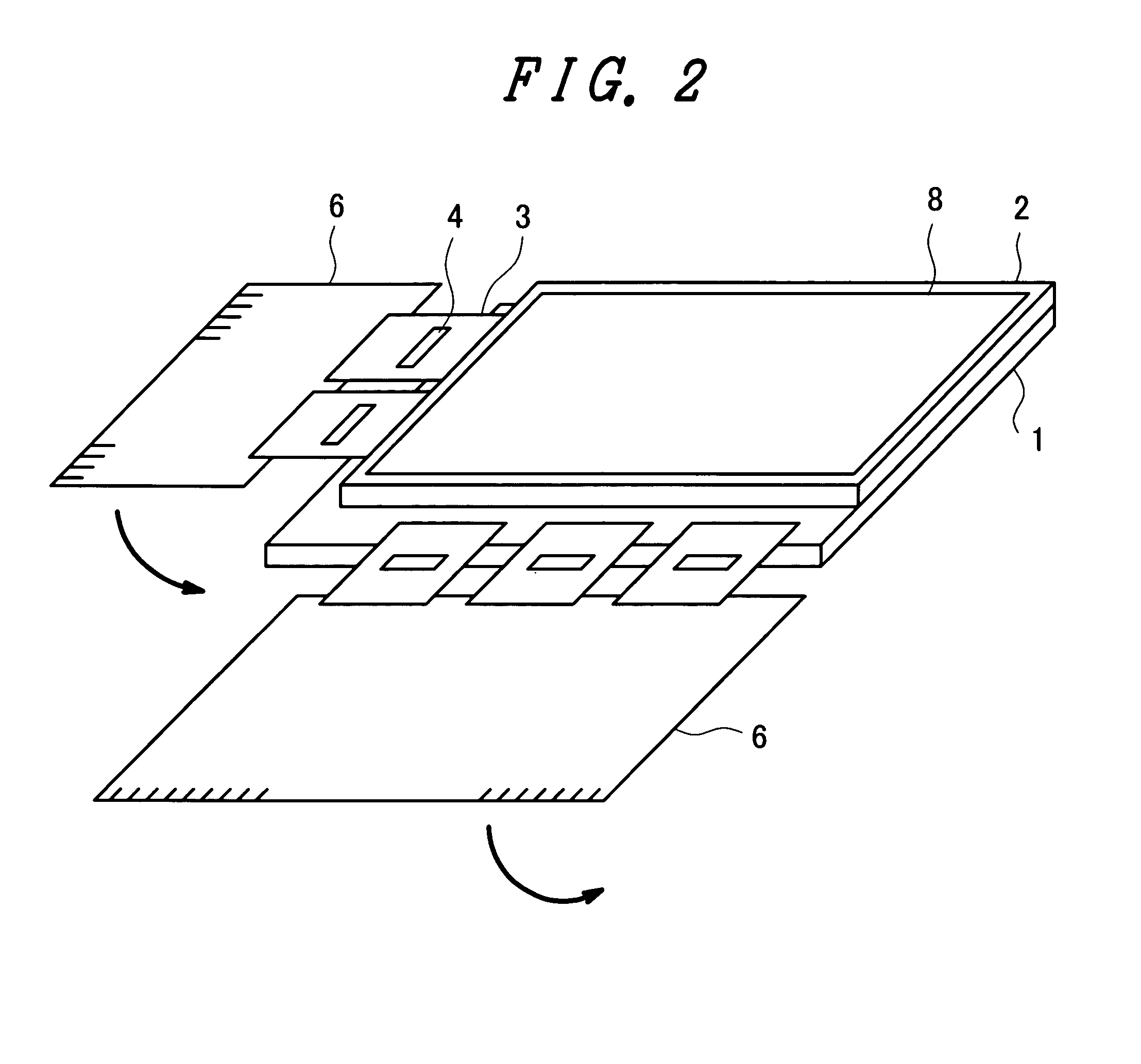
[0068]FIG. 1 shows a TV-use liquid crystal display module as an example to which the present invention is applied. In FIG. 1, a TFT substrate 1 on which pixel electrodes, thin film transistors and the like are arranged in a matrix array and a color filer substrate 2 on which color filters are formed in a matrix array are arranged to overlap each other. Since COFs 3 and the like are mounted on the TFT substrate 1, the TFT substrate 1 is larger than the color filter substrate 2. Here, although COF is an abbreviation of a chip-on-film, in this specification, COF may be also used to imply a COF film. Liquid crystal is sandwiched between the TFT substrate 1 and the color filter substrate 2. An upper polarizer 8 is adhered to an upper surface of the color filter substrate 2, and a lower polarizer (not shown in the drawing) is adhered to a lower surface of the TFT substrate 1. The COF on which an IC chip 4 having a drive circuit is mounted is mounted on two sides of the TFT substrate 1. In...

embodiment 2

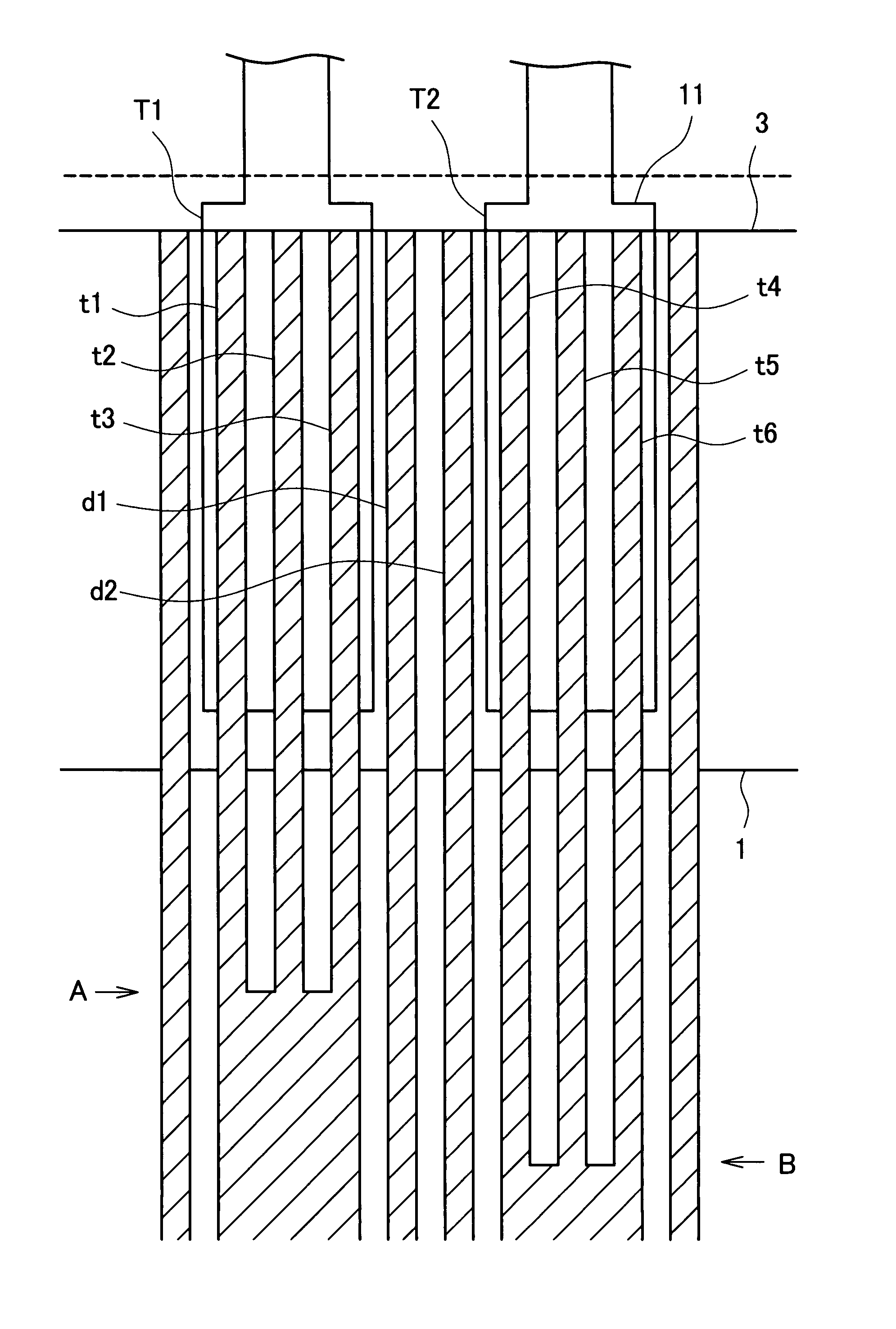
[0094]In the embodiment 1, the explanation is made with respect to the case in which the branching positions of the bold lines are provided in plural number and the branching positions are regularly changed for every line. In the embodiment 2, the explanation is made with respect to the case in which the branching positions are continuously changed for respective neighboring fine lines. In FIG. 13, the respective bold lines on the COF 3 are branched into two fine lines. The branching positions are gradually arranged away from the TFT-substrate-side terminal 34 of the COF 3 such that the branching position of the line P1 is set at a position A, the branching position of the line P2 is set at a position B, and the branching position of the line P3 is set at a position C. By dispersing the branching positions in this manner, it is possible to disperse bending stress when the COF 3 is bent.

[0095]In FIG. 13, although the explanation is made with respect to the case in which the positions...

embodiment 3

[0099]On the COF 3, it is a rare case that the lines are linearly formed from the TFT-substrate-side terminal 34 of the COF 3 to the printed-circuit-board-side terminal 35 of the COF 3 and, in general, the lines are bent in the midst portions thereof. Further, in bending the lines, line widths are also often changed simultaneously. There are various methods for bending the lines in such a case. The simplest way is a method shown in FIG. 16. In this method, as shown in FIG. 16, a line having a width of w1 is bent and, thereafter, the width of the line is changed to w2. In FIG. 16, the width of the fine line before bending is set to a fixed value of w1. Further, the width of the bold line after bending is also set to a fixed value of w2. However, in this case, since the width sharply changes at a bending portion of the line and hence, when the COF 3 is bent, a disconnection is liable to easily occur at a line bending portion, for example, at a portion B shown in FIG. 16, for example. ...


PUM

PropertyMeasurementUnit
thicknessaaaaaaaaaa
thicknessaaaaaaaaaa
thicknessaaaaaaaaaa

Abstract

The present invention prevents, when a COF which is connected with an external circuit is bent in a flat display device, the disconnection of lines on the COF. At a position where a line of the COF is connected to terminal portions of a TFT, and the line having a large width is branched into lines having a small width T1 to T3 or T4 to T6. By displacing line branching positions from each other as indicated by an arrow A and an arrow B, when the COF is bent or deformed, stress applied to the line branching positions can be dispersed thus preventing the disconnection of lines.

Description

[0001]The present application claims priority from Japanese application JP2006-315389 filed on Nov. 22, 2006, the content of which is hereby incorporated by reference into this application.BACKGROUND OF THE INVENTION[0002]1. Field of the Invention[0003]The present invention relates to a display device, and more particularly to the connection structure of a terminal portion and the constitution of a flexible wiring film for establishing an electrical connection of a flat display device with an external circuit.[0004]2. Description of the Related Art[0005]The application of a liquid crystal display device has been spreading from computer monitors, mobile phones and the like to television receiver sets. To drive a liquid crystal display panel, it is necessary to supply a power source, signals and the like to the liquid crystal display panel from the outside. The power source, the signals and the like are often supplied by way of a chip-on-film (COF) which is connected to a terminal por...

Claims


Application Information

Patent Timeline
Patent Type & Authority Patents(United States)
IPC IPC(8): G02F1/1345
CPCH05K1/028H05K3/361G02F1/13452H05K2201/09254H05K2201/09663H01L2924/0002H05K2201/09781H01L2924/00G02F1/1345
Inventor TAKENAKA, YUUICHI
Owner JAPAN DISPLAY INC
Why Eureka
Try Eureka