Eureka AIR delivers breakthrough ideas for toughest innovation challenges, trusted by R&D personnel around the world.

Semiconductor device including a deep contact and a method of manufacturing such a device

Active Publication Date: 2013-06-25
TEXAS INSTR INC
View PDF8 Cites 0 Cited by
  • Summary
  • Abstract
  • Description
  • Claims
  • Application Information

AI Technical Summary

Benefits of technology

The use of polycrystalline silicon has advantages in terms of dopant diffusion and stress conditions for semiconductor devices. The material also allows for higher voltage applications and lower temperatures for uniform doping. Additionally, the combination of polycrystalline silicon with Germanium and / or Carbon can increase reality of the dopant diffusion.

Problems solved by technology

Therefore, the epitaxial thickness cannot always be reduced sufficiently.
This is contrary to the advancements in technology in terms of scaling vertical and lateral dimensions.
Thus, in the state of the art, the further lateral scaling of bipolar transistors is limited by the increasing contact resistance and / or increasing the vertical breakdown voltage is limited by the contact resistance.

Method used


Image

  • Semiconductor device including a deep contact and a method of manufacturing such a device
  • Semiconductor device including a deep contact and a method of manufacturing such a device
  • Semiconductor device including a deep contact and a method of manufacturing such a device

Examples


Embodiment Construction

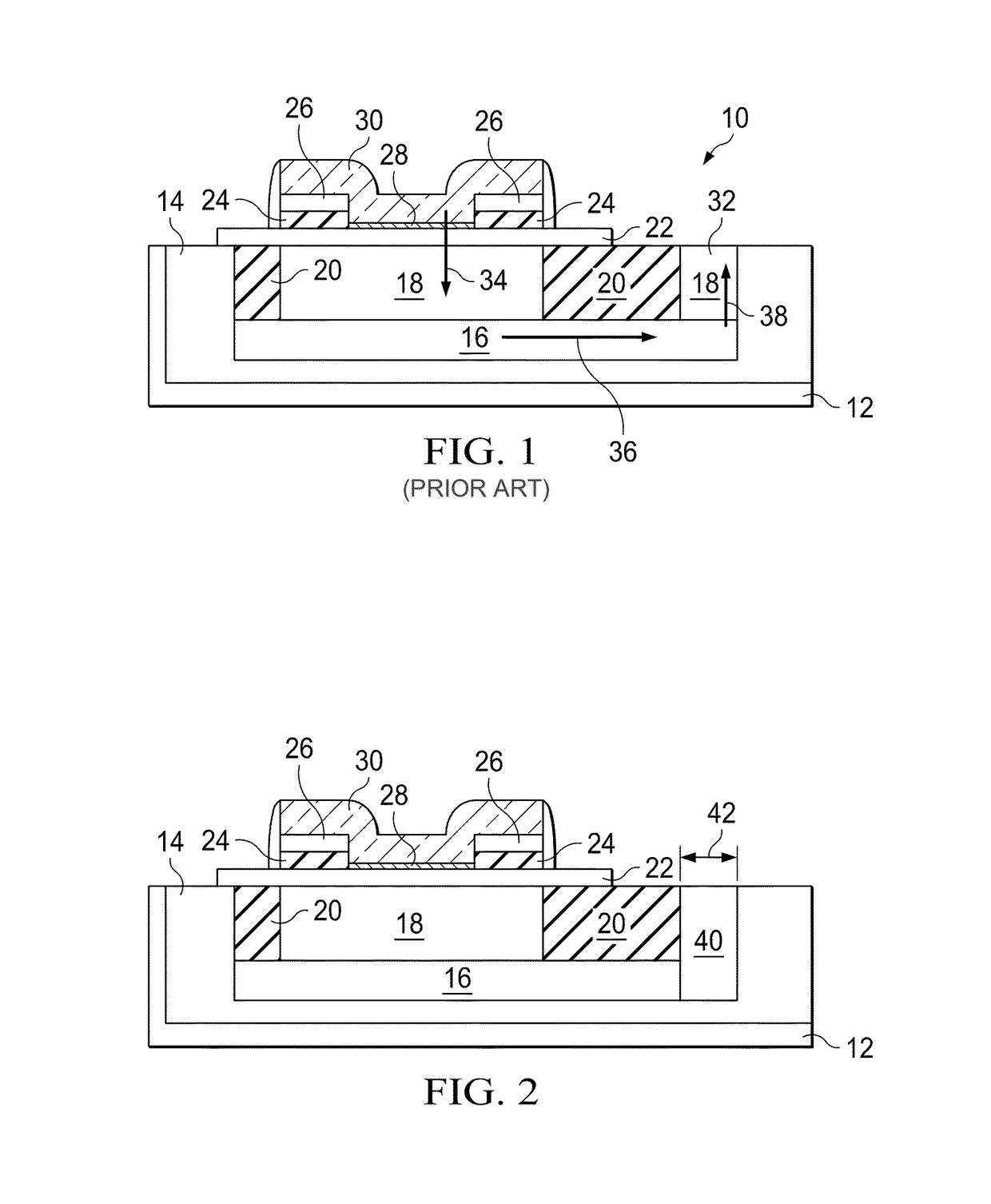
[0028]FIG. 1 shows a conventional PNP transistor device 10. On a substrate 12, a buried layer 16 is formed. On top of the buried layer 16 an active region 18 is formed. Active region 18 is a substantially undoped or lightly doped region. Active region 18 may be formed by any of a variety of techniques well known to those skilled in the art, such as epitaxial growth. The buried layer forms the collector of the bipolar transistor 10. A deep trench isolation 14 is formed, which separates electrically the transistor from neighboring circuitry for example other transistors. Advantageously, an SOI (silicon on insulator) wafer is used and the deep trench isolation goes down to the insulator. In the active region, a shallow trench isolation 20 is formed. Shallow trench isolation is a known technique in the semiconductor technology. For forming the shallow trench isolation, part of the active region is removed, for example, the active region may be epitaxial silicon which is etched away. The...


PUM


Abstract

A semiconductor device includes a buried layer and a deep contact for providing a low resistive connection to the buried layer. The deep contact is formed by doped polycrystalline silicon. A method of manufacturing a semiconductor device and a deep contact for providing a low resistive connection to the buried layer, with the steps of forming a buried layer, providing an active region adjacent the buried layer and forming a deep contact for providing a low resistive connection to the buried layer by patterning a contact shape for the deep contact on an upper surface of the active region, removing part of the active region underneath the contact shape to create a deep contact cavity. Subsequently a polycrystalline silicon layer for filling the deep contact cavity is deposited and doped.

Description

FIELD OF THE INVENTION[0001]The present invention generally relates to a semiconductor device comprising a buried layer and a method of manufacturing such a device.BACKGROUND[0002]It is well-known in the state of the art to manufacture semiconductor devices, for example silicon integrated circuits, which comprise a buried layer. According to the application, the buried layer must be operable to be electrically contacted through an overlaying layer.[0003]A bipolar transistor having a collector formed by a buried layer is an example. The buried layer is usually covered by an epitaxially grown layer of silicon separating the collector from the base of the transistor. The epitaxially grown silicon layer is limited laterally by trenches to form a silicon well.[0004]The collector formed by the buried layer is to be electrically contacted on the upper surface of the device. Therefore, a deep contact providing an electrical connection between the buried layer and the upper surface is needed...

Claims


Application Information

Patent Timeline
IPC IPC(8): H01L21/331
CPCH01L29/0692H01L29/0821H01L29/7322H01L21/76886
Inventor HAEUSLER, ALFRED
Owner TEXAS INSTR INC
Why Eureka
Eureka Blog
Learn More