Fast photolithography process simulation to predict remaining resist thickness

a photolithography and process simulation technology, applied in the field of electronic design automation, can solve the problems of inability to accommodate a large number of process parameters, physical models can be computationally complex to implement, and become more difficult to predict the outcome of such physical and chemical interactions in the process

Active Publication Date: 2013-06-25
SYNOPSYS INC
View PDF5 Cites 2 Cited by
  • Summary
  • Abstract
  • Description
  • Claims
  • Application Information

AI Technical Summary

Benefits of technology

[0010]In various aspects, distribution of exposure energy dose and one or more process variables are applied to the model. The process variables are for physical processes that affect the exposure and / or development of the resist. The post-development (i.e., remaining) thickness of resist at a location on the substrate is computed by using a transfer function that relates exposure energy dose to remaining resist thickness, but which also uses the process variables to account for effects of the other physical processes. This approach can be advantageous because the model is based on the underlying physical processes and therefore potentially performs better compared to purely black box models. On the other hand, the use of a transfer function directly relating exposure energy dose to remaining resist thickness generally requires far less computation than purely physical models.

Problems solved by technology

As the semiconductor fabrication processes become more complex, it is becoming more difficult to predict the outcome of such physical and chemical interactions in the processes.
However, physical models can be computationally complex to implement and may be incapable of accommodating a large number of process parameters that affect the outcome of a fabrication process.
However, the black box model is only as good as the underlying empirical data, and can suffer from inaccuracy when interpolating or extrapolating from available data points.
However, the CTR model is incapable of taking various process parameters into account.
Although the VTR model is more advanced than the CTR model and uses statistical techniques to account for variations caused by various process parameters, the VTR model has less connection to the underlying physical processes associated with the photolithography process and, hence, shows limited accuracy when interpolating and extrapolating.
Furthermore, the VTR model typically is more computationally intensive compared to the CTR model.
However, these models either lack accuracy or require extensive computational resources to simulate the photolithography process.

Method used


Image

  • Fast photolithography process simulation to predict remaining resist thickness
  • Fast photolithography process simulation to predict remaining resist thickness
  • Fast photolithography process simulation to predict remaining resist thickness

Examples


example method

of Optimizing Parameters for a Lithography Model

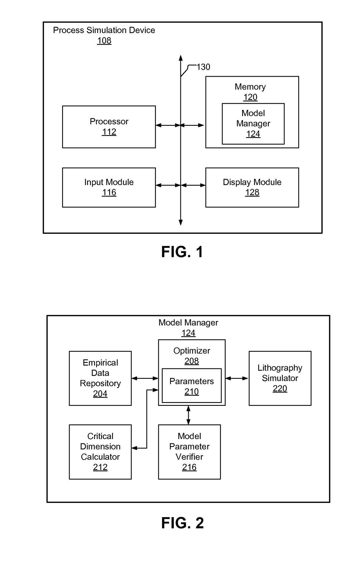
[0053]FIG. 5 is a flowchart illustrating a process of generating parameters for a lithography model, according to one embodiment. The model manager 124 receives 510 an aerial image for forming a test pattern on a wafer. Based on the received aerial image and equation (2), the model manager 124 computes a distribution of exposure energy dose E(x,y) at locations across the wafer.

[0054]The empirical data corresponding to the test pattern are received 514 and stored in the empirical data repository 204. The empirical data may include critical dimensions CDE measured from wafers fabricated to include the test pattern.

[0055]The optimizer 208 initializes 518 the parameters 210 for the lithography model. In one embodiment, the lithography model is represented by equations (3) and (4). The parameters 210 include C0 through CN (for computing Ethresh) and sigmoid slope value a. The critical dimension calculator 212 computes 522 critical dimension...

example simulation

Based on Lithography Model

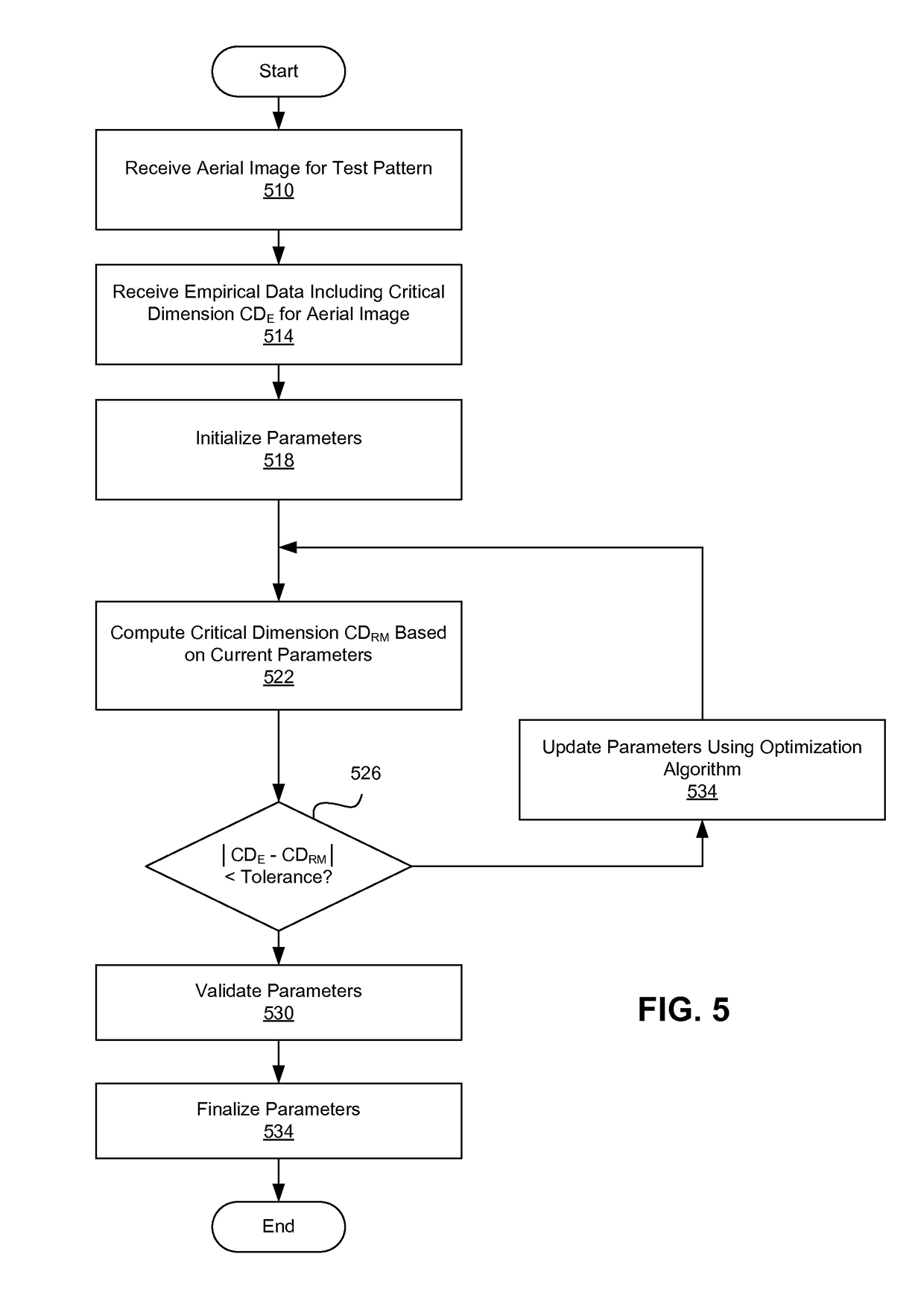
[0066]FIG. 7 is a flowchart illustrating a process of simulating a photolithography process, according to one embodiment. The process of performing simulation using the lithography model is substantially identical to the process of computing the critical dimensions as illustrate in FIG. 6 except that the contour and / or distribution of the remaining resist thickness are obtained as end results instead of the critical dimensions.

[0067]The lithography simulator 220 receives 722 an aerial image for simulation. The lithography simulator 220 computes 724 the exposure energy dose distribution E(x,y) based on the received aerial image and equation (2).

[0068]The lithography simulator 220 also receives 728 the parameters 210 from the optimizer 208. The lithography simulator 220 further receives 732 process variables associated with the simulated photolithography process. Based on the parameters and the process variables, the lithography simulator 220 computes 736 the...


PUM


Abstract

A lithography model uses a transfer function to map exposure energy dose to the thickness of remaining photoresist after development; while allowing the flexibility to account for other physical processes. In one approach, the model is generated by fitting empirical data. The model may be used in conjunction with an aerial image to obtain a three-dimensional profile of the remaining photoresist thickness after the development process. The lithography model is generally compact, yet capable of taking into account various physical processes associated with the photoresist exposure and / or development process for more accurate simulation.

Description

FIELD OF THE INVENTION[0001]The present invention is related to electronic design automation (EDA) for simulating resist exposure and development during an integrated circuit fabrication process. More specifically, it relates to a fast lithography model that predicts the thickness of remaining resist.BACKGROUND OF THE INVENTION[0002]Semiconductor integrated circuit (IC) fabrication processes involve complex physical and chemical interactions. As the semiconductor fabrication processes become more complex, it is becoming more difficult to predict the outcome of such physical and chemical interactions in the processes. Process models are developed to predict the outcome of these processes. Process models may be a physical model, a black box model or a combination of both. A physical model is based on an understanding of the actual physical processes that occur during a fabrication process and attempts to simulate those processes. Conversely, a black box model is typically a statistica...

Claims


Application Information

Patent Timeline
Patent Type & Authority Patents(United States)
IPC IPC(8): G06F17/50
CPCG03F7/705G03F7/70666
Inventor ISOYAN, ARTAKMELVIN, III, LAWRENCE S.
Owner SYNOPSYS INC
Why Eureka
Try Eureka