
Measurement model optimization based on parameter variations across a wafer
a measurement model and parameter variation technology, applied in the field ofmetrology systems and methods, can solve the problems of optical radiation reaching the bottom layer, characterization difficulty, and characterization becomes more difficult, so as to reduce the computation time of library generation, less correlation among parameters, and accurate measurement results
- Summary
- Abstract
- Description
- Claims
- Application Information
AI Technical Summary
Benefits of technology
Problems solved by technology
Method used
Image

Examples
Embodiment Construction
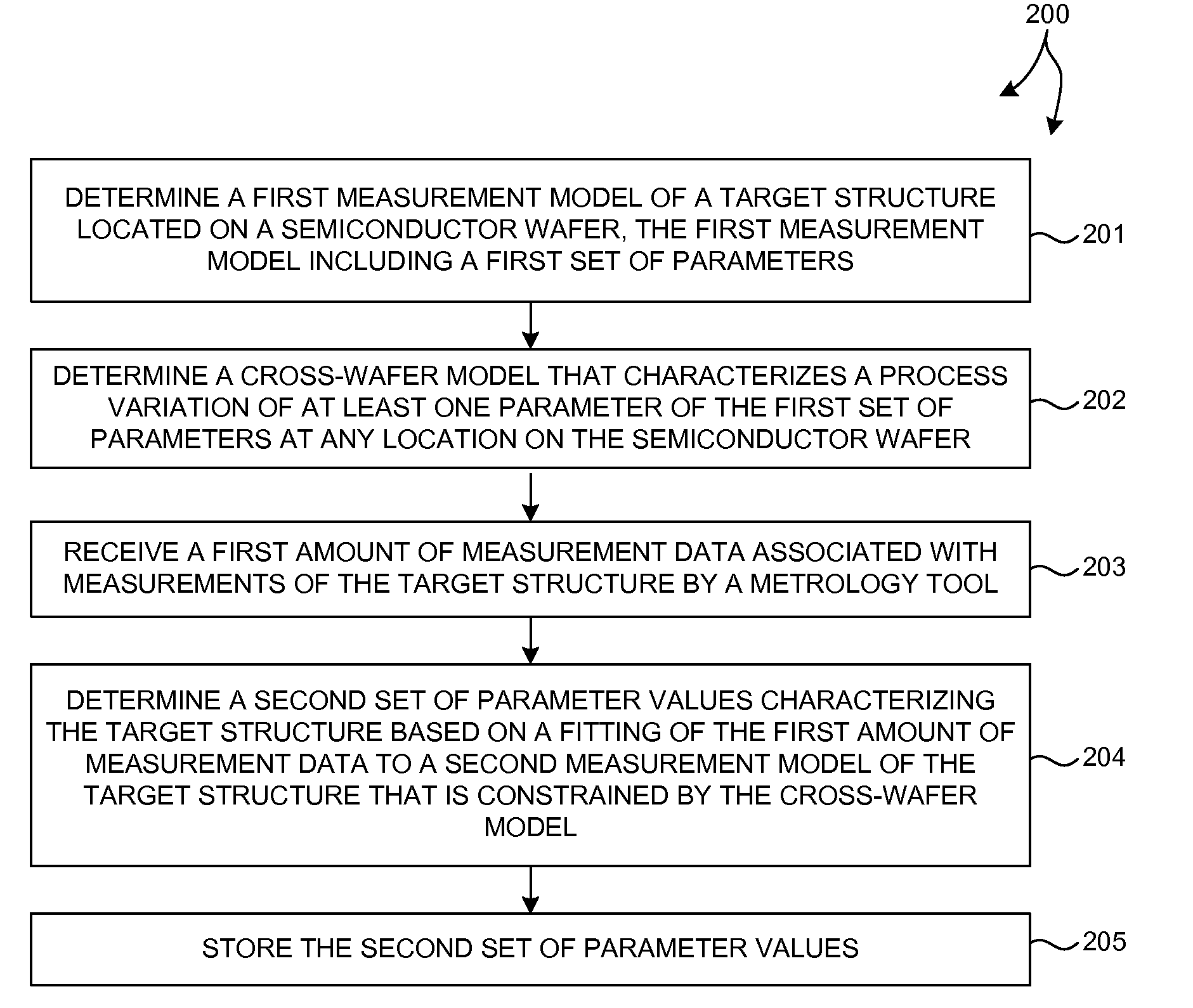
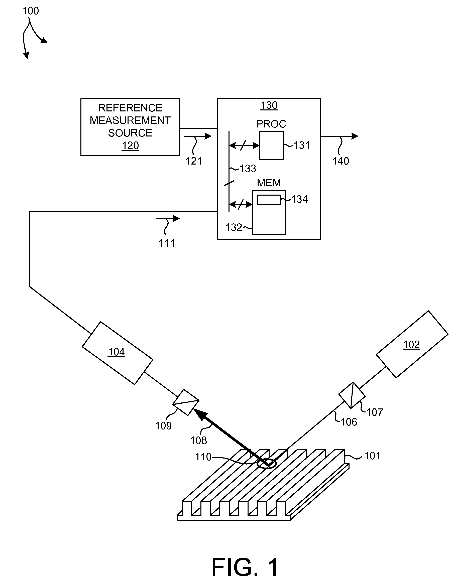
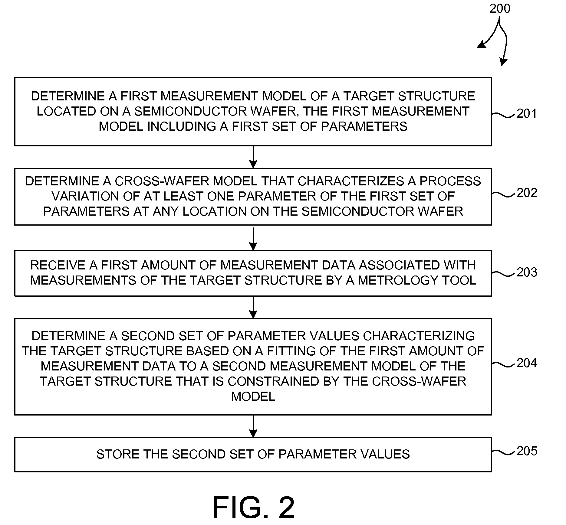
[0020]Reference will now be made in detail to background examples and some embodiments of the invention, examples of which are illustrated in the accompanying drawings. Methods and systems for optimizing measurement models based on modeling of parameter variations across a semiconductor wafer are presented. Systems employing optimized measurement models are used to measure structural and material characteristics (e.g., material composition, dimensional characteristics of structures and films, etc.) associated with different semiconductor fabrication processes.
[0021]In general, optical metrology techniques discussed herein are indirect methods of measuring physical properties of a specimen under inspection. In most cases, the measured values cannot be used to directly determine the physical properties of the specimen. The nominal measurement process consists of parameterization of the structure (e.g., film thicknesses, critical dimensions, etc.) and the machine (e.g., wavelengths, an...
PUM
 Abstract
Description
Claims
Application Information