Measurement Model Optimization Based On Parameter Variations Across A Wafer

a measurement model and parameter variation technology, applied in the field ofmetrology systems and methods, can solve the problems of optical radiation reaching the bottom layer, characterization difficulty, and characterization becomes more difficult, so as to reduce the computation time of library generation, less correlation among parameters, and accurate measurement results

Active Publication Date: 2013-11-14
KLA TENCOR TECH CORP
View PDF2 Cites 25 Cited by
  • Summary
  • Abstract
  • Description
  • Claims
  • Application Information

AI Technical Summary

Benefits of technology

[0014]The measurement model is constrained by the cross-wafer model of parameter variations. In this manner, the set of parameters that must be fitted to arrive at a measurement solution is reduced. This results in less correlation among parameters, more accurate measurement results, and less computation time for library generation, fitting, and analysis. For example, correlation between the thickness of layers and a grating structure fabricated on top of the layers is eliminated or significantly reduced. Accuracy is improved because the modeled parameters are floated and constrained across the wafer instead of fixed to some nominal value. In some examples, the optimized measurement model enables measurements with fewer measurement technologies and reduced range of illumination wavelengths to achieve satisfactory measurement results. In some examples, measurement systems employing high intensity light sources within limited wavelength ranges is enabled by the optimized measurement model.

Problems solved by technology

As devices (e.g., logic and memory devices) move toward smaller nanometer-scale dimensions, characterization becomes more difficult.
Devices incorporating complex three-dimensional geometry and materials with diverse physical properties contribute to characterization difficulty.
For example, modern memory structures are often high-aspect ratio, three-dimensional structures that make it difficult for optical radiation to penetrate to the bottom layers.
As a result, the measurement model parameters characterizing the target often cannot be reliably decoupled.
In response to these challenges, more complex optical tools have been developed.
In addition, the spreading of light intensity over large wavelength ranges decreases illumination intensity at any particular wavelength and increases signal uncertainty of measurements performed at that wavelength.
Future metrology applications present challenges for metrology due to increasingly small resolution requirements, multi-parameter correlation, increasingly complex geometric structures, and increasing use of opaque materials.
In some examples, the cross-wafer model gives rise to constraints on the relationships among unknown specimen parameters based on location on the wafer.

Method used


Image

  • Measurement Model Optimization Based On Parameter Variations Across A Wafer
  • Measurement Model Optimization Based On Parameter Variations Across A Wafer
  • Measurement Model Optimization Based On Parameter Variations Across A Wafer

Examples


Embodiment Construction

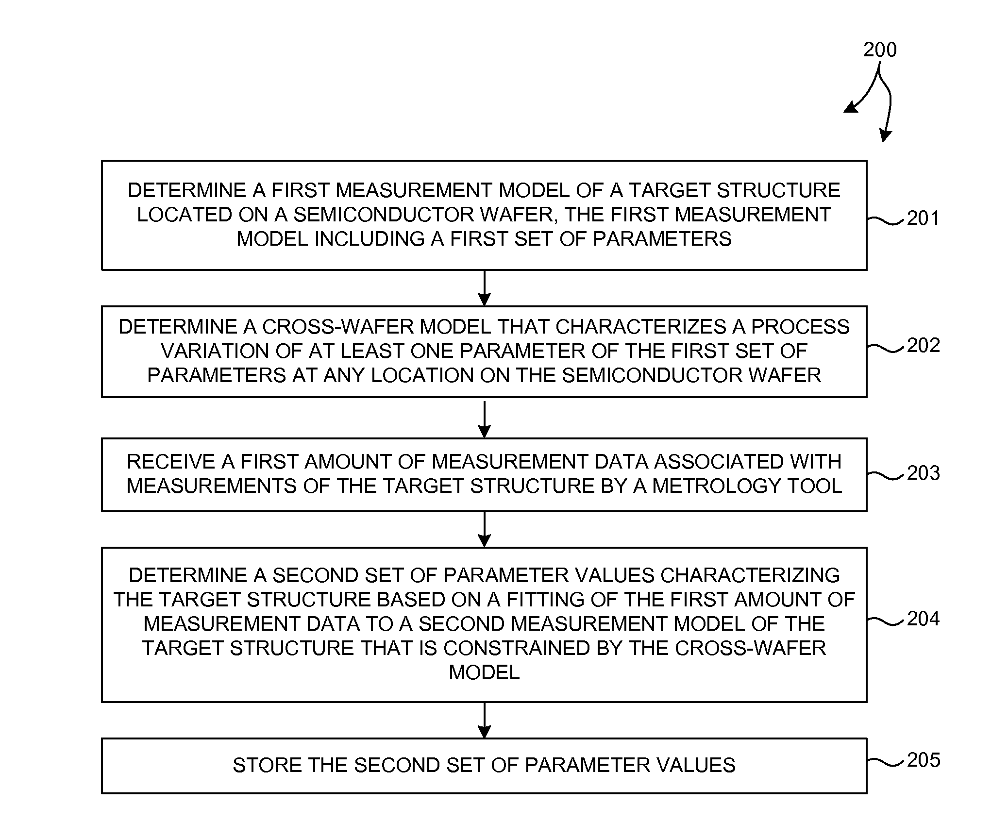
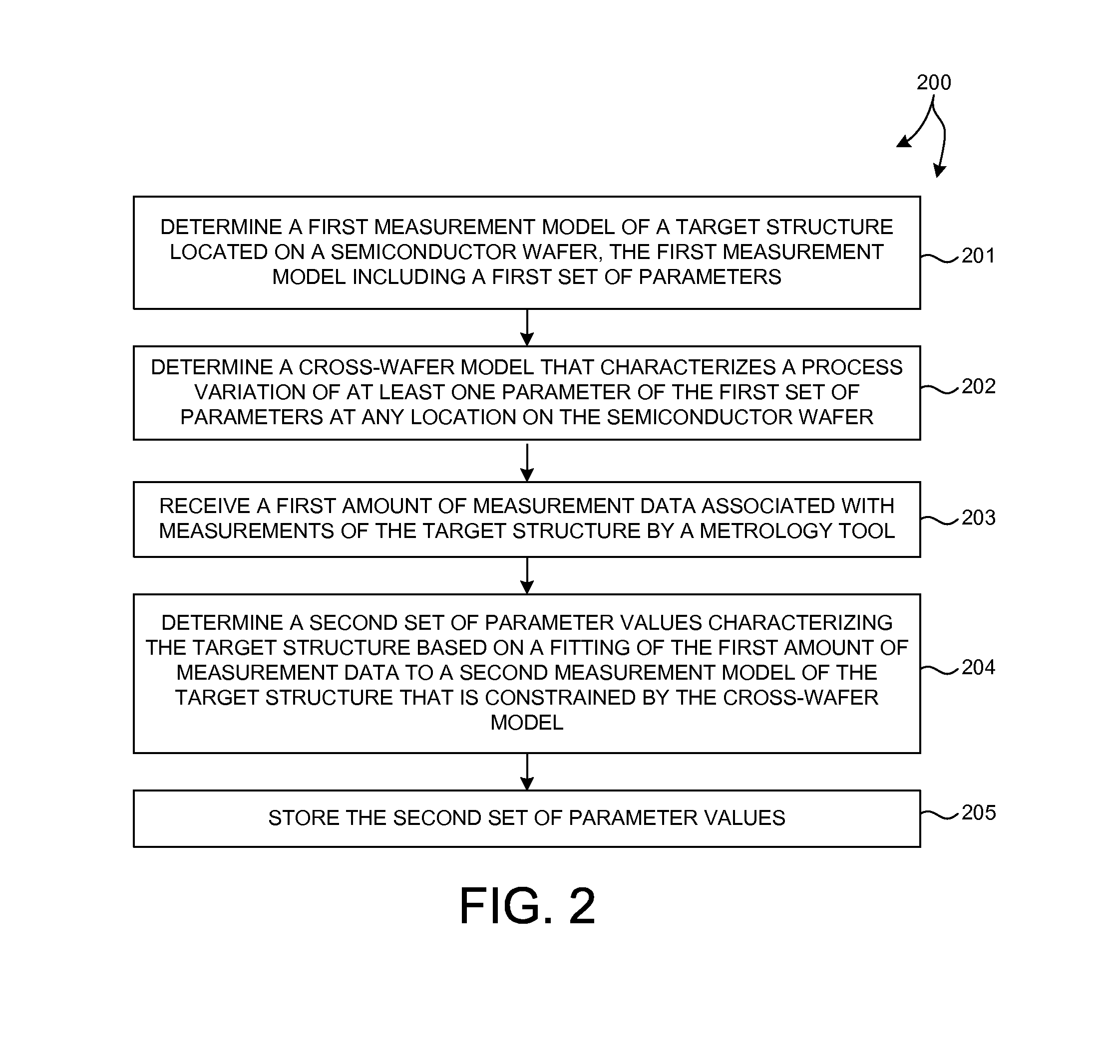
[0020]Reference will now be made in detail to background examples and some embodiments of the invention, examples of which are illustrated in the accompanying drawings. Methods and systems for optimizing measurement models based on modeling of parameter variations across a semiconductor wafer are presented. Systems employing optimized measurement models are used to measure structural and material characteristics (e.g., material composition, dimensional characteristics of structures and films, etc.) associated with different semiconductor fabrication processes.

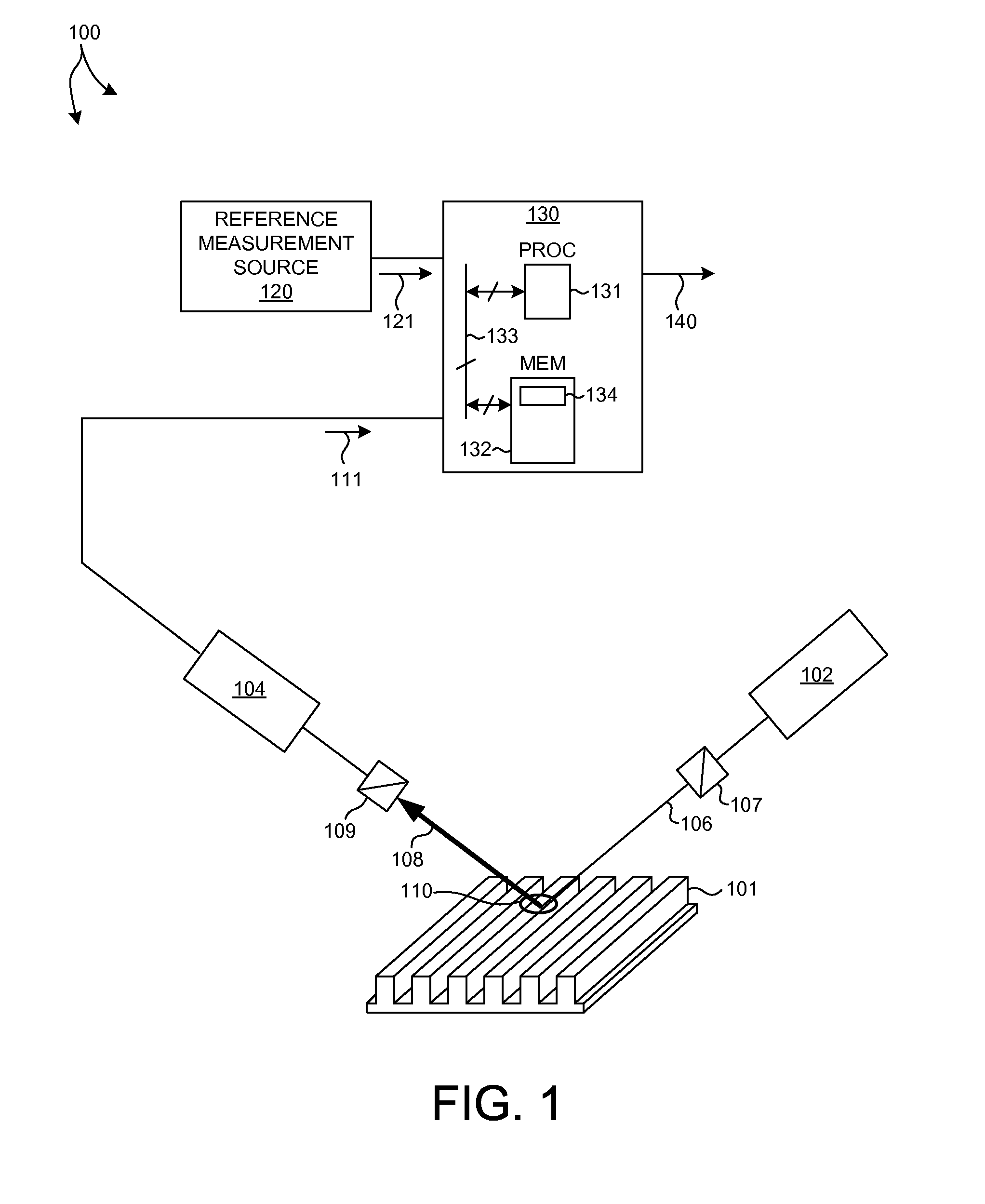
[0021]In general, optical metrology techniques discussed herein are indirect methods of measuring physical properties of a specimen under inspection. In most cases, the measured values cannot be used to directly determine the physical properties of the specimen. The nominal measurement process consists of parameterization of the structure (e.g., film thicknesses, critical dimensions, etc.) and the machine (e.g., wavelengths, an...


PUM


Abstract

An optimized measurement model is determined based a model of parameter variations across a semiconductor wafer. A global, cross-wafer model characterizes a structural parameter as a function of location on the wafer. A measurement model is optimized by constraining the measurement model with the cross-wafer model of process variations. In some examples, the cross-wafer model is itself a parameterized model. However, the cross-wafer model characterizes the values of a structural parameter at any location on the wafer with far fewer parameters than a measurement model that treats the structural parameter as unknown at every location. In some examples, the cross-wafer model gives rise to constraints among unknown structural parameter values based on location on the wafer. In one example, the cross-wafer model relates the values of structural parameters associated with groups of measurement sites based on their location on the wafer.

Description

CROSS REFERENCE TO RELATED APPLICATION[0001]The present application for patent claims priority under 35 U.S.C. §119 from U.S. provisional patent application Ser. No. 61 / 644,030, entitled “Process Based Cross Wafer Model Optimization,” filed May 8, 2012, the subject matter of which is incorporated herein by reference in its entirety.TECHNICAL FIELD[0002]The described embodiments relate to metrology systems and methods, and more particularly to methods and systems for improved measurement of structural parameters.BACKGROUND INFORMATION[0003]Semiconductor devices such as logic and memory devices are typically fabricated by a sequence of processing steps applied to a specimen. The various features and multiple structural levels of the semiconductor devices are formed by these processing steps. For example, lithography among others is one semiconductor fabrication process that involves generating a pattern on a semiconductor wafer. Additional examples of semiconductor fabrication process...

Claims


Application Information

Patent Timeline
Patent Type & Authority Applications(United States)
IPC IPC(8): G06F17/50
CPCG06F17/5081H01L22/20H01L22/12H01L2924/0002H01L2924/00G06F30/398
Inventor PANDEV, STILIAN IVANOV
Owner KLA TENCOR TECH CORP
Why Eureka
Try Eureka