

Formed PCB
a pcb and bending technology, applied in the field of pcb, can solve the problems of unused dead space within the device, and achieve the effects of increasing the overall stiffness of the pcb, reducing the risk of bending, and being more resistant to bending
- Summary
- Abstract
- Description
- Claims
- Application Information
AI Technical Summary
Benefits of technology
Problems solved by technology
Method used
Image

Examples
Embodiment Construction
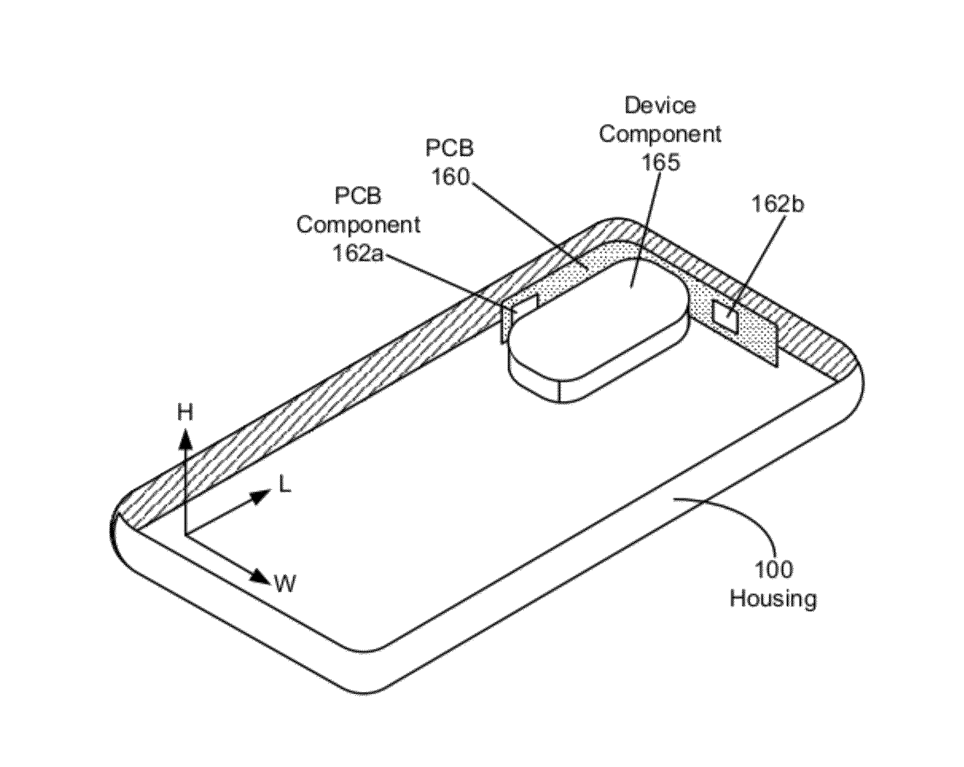
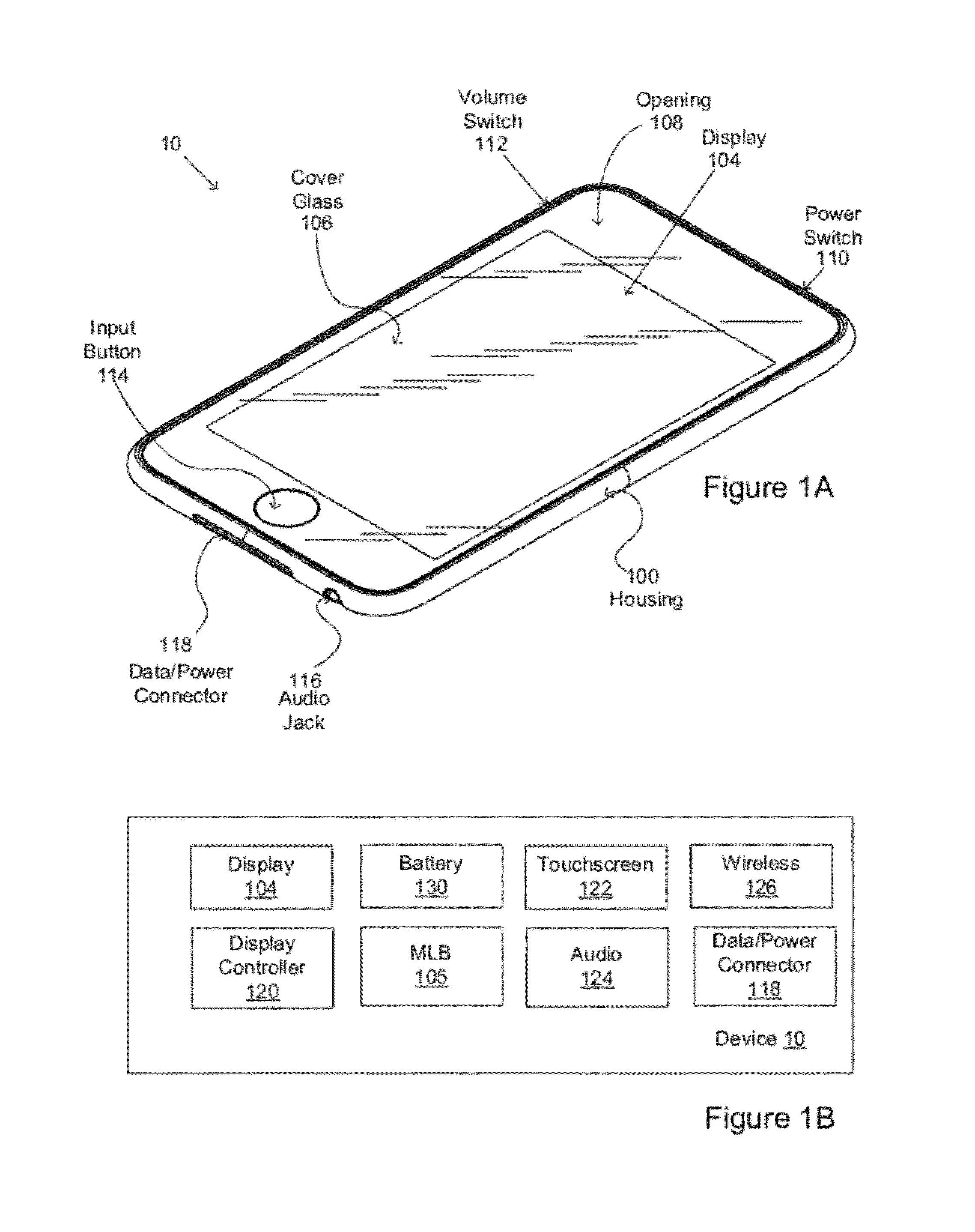
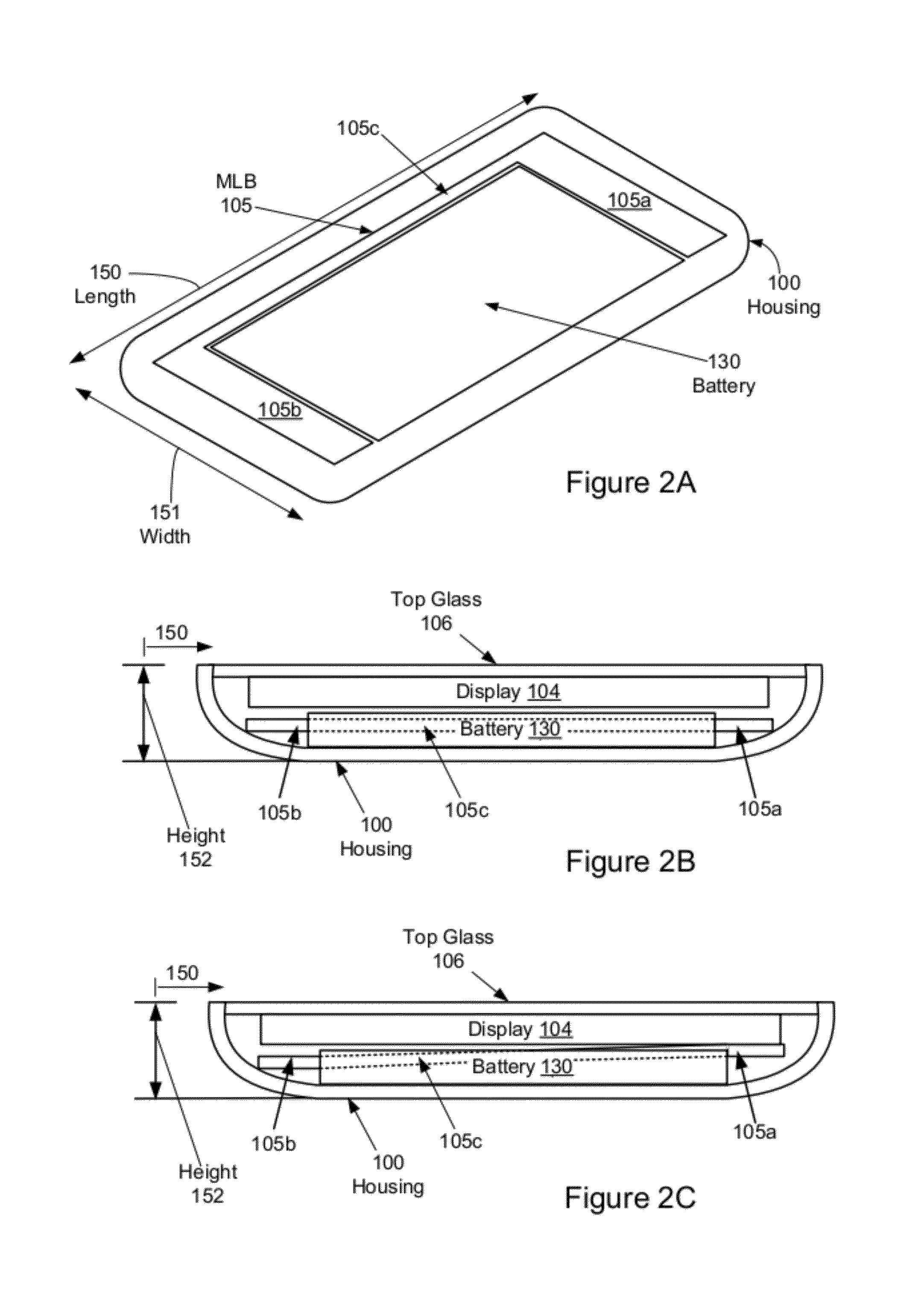
[0002]The described embodiments relate generally to computing devices such as laptop computers, tablet computers, and the like. More particularly, internal packaging architectures involving printed circuit board design are described.
[0003]2. Description of the Related Art
[0004]In recent years, portable computing devices such as laptops, PDAs, media players, cellular phones, etc., have become small, light and powerful. One factor contributing to this reduction in size can be attributed to the manufacturer's ability to fabricate various components of these devices in smaller and smaller sizes while in most cases increasing the power and or operating speed of such components. Another factor contributing to the reduction in size is that from a visual stand point, users often find compact and sleek designs of consumer electronic devices more aesthetically appealing and thus, demand compact and sleek designs. The trend of smaller, lighter, more compact and powerful presents continuing cha...
PUM
| Property | Measurement | Unit |
|---|---|---|
| angle | aaaaa | aaaaa |
| heights | aaaaa | aaaaa |
| power | aaaaa | aaaaa |
Abstract
Description
Claims
Application Information