Package structure and electronic apparatus of the same

a technology of electronic equipment and packaging, applied in the field of packaging, can solve the problems of inconvenient design of printed circuit boards b, client end, and the entire package process will become more difficult, and achieve the effects of reducing the difficulty of the package process, and simplifying the design of printed circuit boards

Active Publication Date: 2013-07-02
AMAZING MICROELECTRONICS
View PDF7 Cites 2 Cited by
  • Summary
  • Abstract
  • Description
  • Claims
  • Application Information

AI Technical Summary

Benefits of technology

[0019]Above all, a package structure having interlaced pins and an electronic apparatus including the package structure of the invention can increase the minimum spacing between the adjacent pins in the package structure to lower the difficulty of the package process. In addition, since the routing of the printed circuit board can directly penetrate the bottom of the package structure, therefore, the design of the printed circuit board will become simpler and easier. It should be noticed that the package structure and the electronic apparatus including the package structure of the invention can provide obvious improvement to the circuits sensitive to loads or layout (e.g., a high-speed signal circuit).

Problems solved by technology

When the minimum spacing limitation becomes smaller and smaller, the entire package process will become more difficult.
Moreover, since each pin disposed on the printed circuit board 10 must be bended to dodge the opposite pin, the routings of the printed circuit board 10 fail to penetrate the bottom of the package structure 1, therefore, it is quite inconvenient to the design of the printed circuit board 10 of the client end.

Method used


Image

  • Package structure and electronic apparatus of the same
  • Package structure and electronic apparatus of the same
  • Package structure and electronic apparatus of the same

Examples


first embodiment

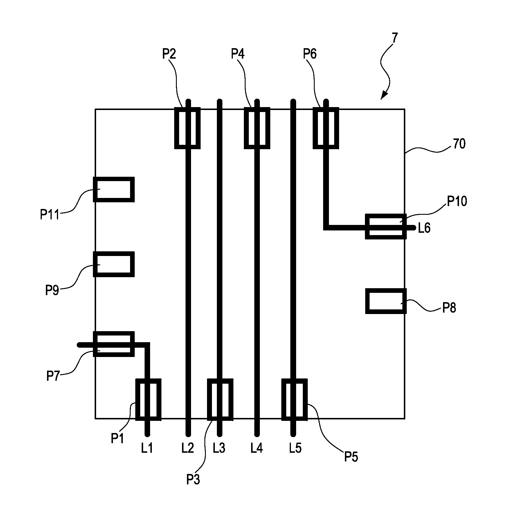
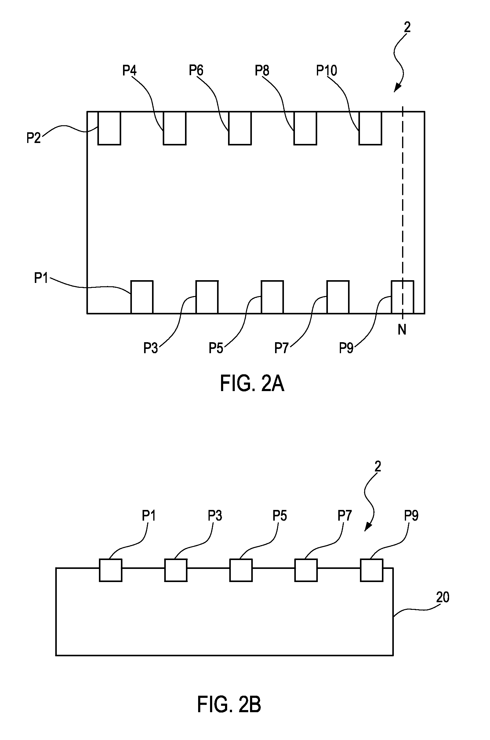
[0034]the invention is a package structure of the printed circuit board. Please refer to FIG. 2A. FIG. 2A shows a scheme diagram of the package structure. As shown in FIG. 2A, the package structure 2 includes a substrate 20 and pins P1˜P10. The pins P1˜P10 are disposed on the substrate 20. The pins P1˜P10 are interlaced to each other, so that a straight line along a specific direction (namely the direction vertical to the two sides of the pin disposed on the substrate 20, but not limited to this) will only pass one of the pins P1˜P10 at most. That is to say, among the pins P1˜P10, no any two pins will be disposed at the same straight line along the specific direction. For example, the straight line N in FIG. 2A will only pass the pin P9 of the pins P1˜P10 instead of passing other pins.

[0035]More specifically, as shown in FIG. 2A, the pins P1, P3, P5, P7, and P9 in the package structure 2 are disposed at a first side of the substrate 20, and the pins P2, P4, P6, P8, and P10 are dispo...

second embodiment

[0049]A second embodiment according to the invention is an electronic apparatus. In this embodiment, the electronic apparatus includes a package structure. The package structure includes a substrate and a plurality of pins. The plurality of pins is disposed on the substrate. The plurality of pins is interlaced to each other, so that a line along a specific direction will only pass one of the plurality of pins at most.

[0050]In practical applications, the plurality of pins can further include a plurality of first pins and a plurality of second pins. The plurality of first pins and the plurality of second pins are disposed at a first side and a second side of the substrate respectively. The plurality of first pins and the plurality of second pins are interlaced to each other.

[0051]In addition, the plurality of pins can further include a plurality of third pins, the plurality of third pins is disposed between the first side and the second side of the substrate, and the plurality of thir...


PUM


Abstract

A package structure and an electronic apparatus of the package structure are disclosed. The package structure includes a substrate and a plurality of pins. The plurality of pins is disposed on the substrate. The plurality of pins is interlaced to each other, so that a line along a specific direction will only pass one of the plurality of pins at most.

Description

CROSS-REFERENCE TO RELATED APPLICATION[0001]This application claims the benefit of Taiwan Patent Application No. 099204040, filed on Mar. 8, 2010, which is hereby incorporated by reference for all purposes as if fully set forth herein.BACKGROUND OF THE INVENTION[0002]1. Field of the Invention[0003]The invention relates to package. In particular, the invention relates to a package structure having interlaced pins and an electronic apparatus including such package structure could increase the minimum spacing between the adjacent pins to lower the difficulty of the package process. In addition, since the routing of the printed circuit board can directly penetrate the bottom of the package structure, therefore, the design of the printed circuit board will become simpler and easier. Especially, the circuits sensitive to loads or layout (e.g., a high-speed signal circuit) will be deeply affected.[0004]2. Description of the Prior Art[0005]In recent years, with the innovation and developmen...

Claims


Application Information

Patent Timeline
Patent Type & Authority Patents(United States)
IPC IPC(8): H01R9/00
CPCH05K1/00H01L23/49838H01L2924/0002H01L2924/00
Inventor LIN, HO-SHYANWONG, TSU-YANG
Owner AMAZING MICROELECTRONICS
Why Eureka
Try Eureka