Tall mezzanine connector

a connector and flexible technology, applied in the direction of electrical apparatus, coupling device connection, printed circuit, etc., can solve the problems of limiting the maximum electrical transmission distance, limiting the speed at which signals can be transmitted, and using electrical chip-to-chip signaling, etc., to reduce the length of the signal path, reduce the amount of misalignment, and reduce the amount of wire density

Inactive Publication Date: 2013-07-16
GLOBALFOUNDRIES INC
View PDF37 Cites 24 Cited by
  • Summary
  • Abstract
  • Description
  • Claims
  • Application Information

AI Technical Summary

Benefits of technology

[0025]The tall flexible mezzanine connector of the present invention is configured in such a way that there is compliance in the connector that allows it to mate to another half of the connector when the two halves do not align. This compliance allows the connector to be taller, on the order of 100 mm or more, because as distances between boards increase the amount of misalignment increases. A secondary benefit of this invention is that it can be made to be soldered onto surface pads or to be attached to a circuit board by means of a land grid array as opposed to pins pressed into the circuit board. This allows more dense wiring underneath the connector. Another benefit of this invention is, because of the compliance of the connector with respect to the two circuit cards being connected together, more than one connector can be used between two circuit cards and there is no limitation as to the location of one connector with respect to another. This allows a great deal of flexibility in the design of circuits traveling between two circuit cards to minimize signal path lengths and maximize the frequency of signals traveling between the two cards.
[0026]More specifically, the present invention is a connector comprising a flexible wafer assembly having means for connecting at least two electronic circuit boards, at any location along the two electronic circuit boards. The connector of wafer assemblies possesses a solid connector substrate having edges defining a shape of the connector substrate and at least one conductive layer in the connector substrate containing signal layers extending from a first edge of the solid substrate to a second edge of the solid substrate; and a return current path ground means for providing a constant impedance and effective shielding between the signal conductors. The flexibility of the connector provides the compliance noted above by allowing the connector to twist or bend in order to connect two distinct circuit cards which are not situated in direct alignment with each other. The wafer assemblies in the connector have built-in flexibility so that the connector can assume a curved or angular shape as discussed in greater detail below.

Problems solved by technology

The patented prior art cited above has become less pertinent because, as computers have become faster, i.e., as communications data rates have increased, transmission line impedance discontinuities and frequency-dependent channel loss have limited the maximal electrical transmission distance.
The result is that the net lengths of the computer limit the speed at which signals can be transmitted.
A more serious limit on the use of electrical chip-to-chip signaling has been the lack of a sufficiently reliable, separable and dense electrical card-to-card connection technology.
As a result recent large-scale computing systems have trended towards signaling electrically over the largest possible circuit card, and using dense but expensive optical interconnections between circuit cards.
This limitation forces all signals leaving the card to be carried to another card to connect to this particular edge.
The prior art articles are unsuitable for this application.
The limitation of these existing connectors is their height.

Method used


Image

  • Tall mezzanine connector
  • Tall mezzanine connector
  • Tall mezzanine connector

Examples


Embodiment Construction

[0074]The preferred embodiment of the present invention will be described below with reference to the accompanying drawings.

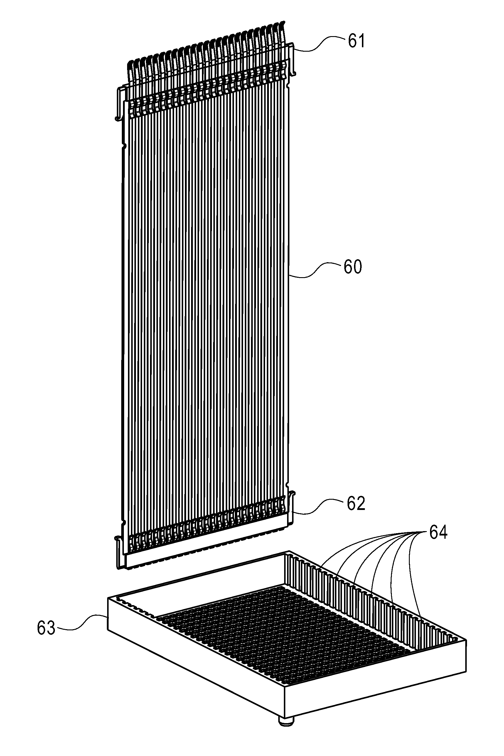
[0075]The tall mezzanine connector of the present invention inter alia, connects two parallel circuit boards.

[0076]More particularly, the wafer connector substrate in the preferred embodiment is a rectangular cuboid since it is a three-dimensional solid, however the wafer connector can assume the shape of any prism configuration depending upon the application to which the wafer connector is to be put.

[0077]In describing the present invention, the term “connector” as used herein encompasses a header and a receptacle. The “header” is comprised of a header-base and a plurality of pin assemblies. The “receptacle” is comprised of a receptacle bottom-base, a plurality of wafer assemblies and a top base. The expression “wafer assembly” comprises a wafer circuit card, an upper contact finger assembly and a lower contact finger assembly. Further, as used herein, “wafer ...


PUM


Abstract

A tall mezzanine connector which connects the substantial middle half of each of a pair of circuit cards positioned normal thereto in such a way that there is compliance when the two halves of the circuit cards are not in alignment. The mezzanine connector comprises a header and a receptacle that includes wafers having electrical contact means at each end thereof for contacting contacts in the respective circuit cards, the wafers being held in place by an upper base member and a lower base member.

Description

BACKGROUND OF THE INVENTION[0001]1. Field of the Invention[0002]The invention relates to reliable, separable and dense electrical card-to-card connection technology that is used to make a plurality of electrical connections across the area of large circuit boards. More specifically, the invention relates to a tall, flexible mezzanine connector for parallel-mounted or normal positioned cards.[0003]2. Background of the Invention[0004]The need for chip-to-chip communication bandwidth has tracked the increasing circuit density and computational power of Integrated Circuit (IC) chips. This increased bandwidth has been provided both by increasing the number of chip-to-chip interconnections and by increasing the data rate per interconnection. In computer networks, bandwidth is often used as a synonym for data transfer rate—the amount of data that can be carried from one point to another in a given time period (usually a second). This kind of bandwidth is usually expressed in bits (of data)...

Claims


Application Information

Patent Timeline
Patent Type & Authority Patents(United States)
IPC IPC(8): H01R12/00
CPCH01R13/514H01R13/6587
Inventor CIPOLLA, THOMAS M.TAKKEN, TODDCOTEUS, PAUL W.
Owner GLOBALFOUNDRIES INC
Why Eureka
Try Eureka