Resin sealing type semiconductor device and method of manufacturing the same, and resin sealing type electronic device

a technology of electronic devices and sealing types, which is applied in semiconductor devices, semiconductor/solid-state device details, electrical devices, etc., can solve the problems of short-circuiting outer, affecting the welding performance of the semiconductor device, and the plated silver is also unstably plated on the small lead burrs

Active Publication Date: 2013-08-06
SEMICON COMPONENTS IND LLC
View PDF12 Cites 0 Cited by
  • Summary
  • Abstract
  • Description
  • Claims
  • Application Information

AI Technical Summary

Benefits of technology

[0068]By the method of manufacturing the resin sealing type semiconductor device of the invention, the resin sealing type semiconductor device with high reliability is manufactured by preventing the mustache-like solder burr 12 caused by the lead burr 10 formed on the lead frame 1 by presswork.
[0013]The invention also provides a resin sealing type electronic device that includes a lead having an electronic component mounting surface and a welding surface opposite from the component mounting surface. The electronic component mounting surface includes a plurality of burrs standing thereon as a result of punching a metal board using a mold from the welding surface. The device also includes an electronic component bonded to the electronic mounting surface of the lead, a resin package sealing the electronic component and the lead so that a part of the lead is exposed from the package, and an external electrode on which a portion of the welding surface of the exposed lead is welded.

Problems solved by technology

These lead burrs cause the following problems in a resin sealing type semiconductor device and so on and a process of manufacturing the same, and a resin sealing type electronic device.
In the case of the solder plating, a solder plating layer is formed on all of the outer leads, and the solder is also unstably plated on the small lead burrs formed by the presswork.
In the subsequent process of cutting the tie bars, this solder plating layer applied to the small lead burrs peels off to form mustache-like solder burrs, thereby causing a problem of short-circuiting the outer leads and so on.
In this case, due to the protruding lead burrs described above, the surface of the outer lead and the surface of the external electrode are not bonded firmly and a welding failure is likely to occur.
On the other hand, in a case of bonding an electronic component to an inner lead inside the resin package, since the opposite surface to the lead burr formation surface forms a rounded surface of which the ends are rounded, when an electronic component is bonded to the rounded surface, there occurs a problem that the bonding area is small to cause a connection failure and so on.

Method used


Image

  • Resin sealing type semiconductor device and method of manufacturing the same, and resin sealing type electronic device
  • Resin sealing type semiconductor device and method of manufacturing the same, and resin sealing type electronic device
  • Resin sealing type semiconductor device and method of manufacturing the same, and resin sealing type electronic device

Examples


first embodiment

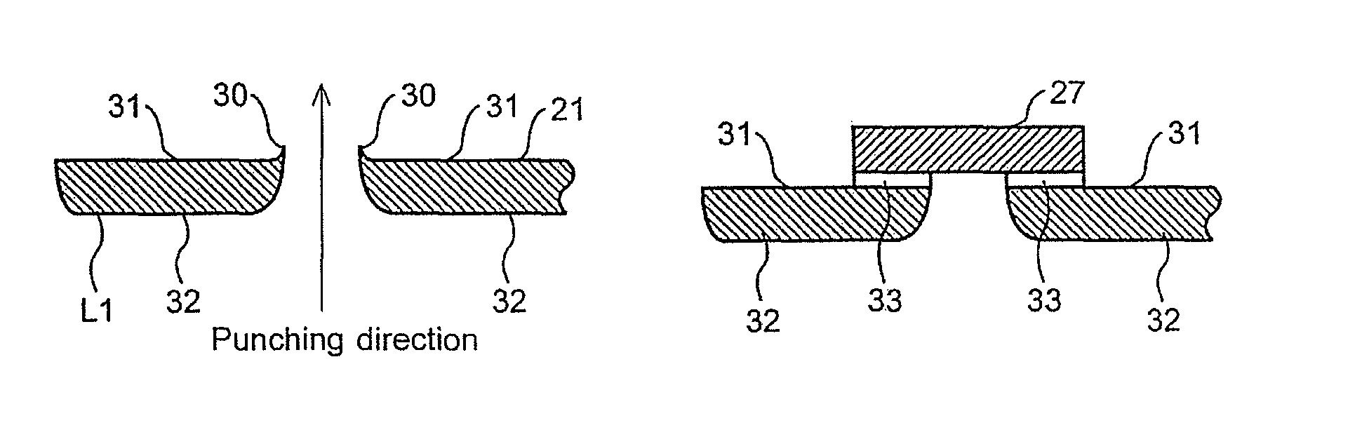
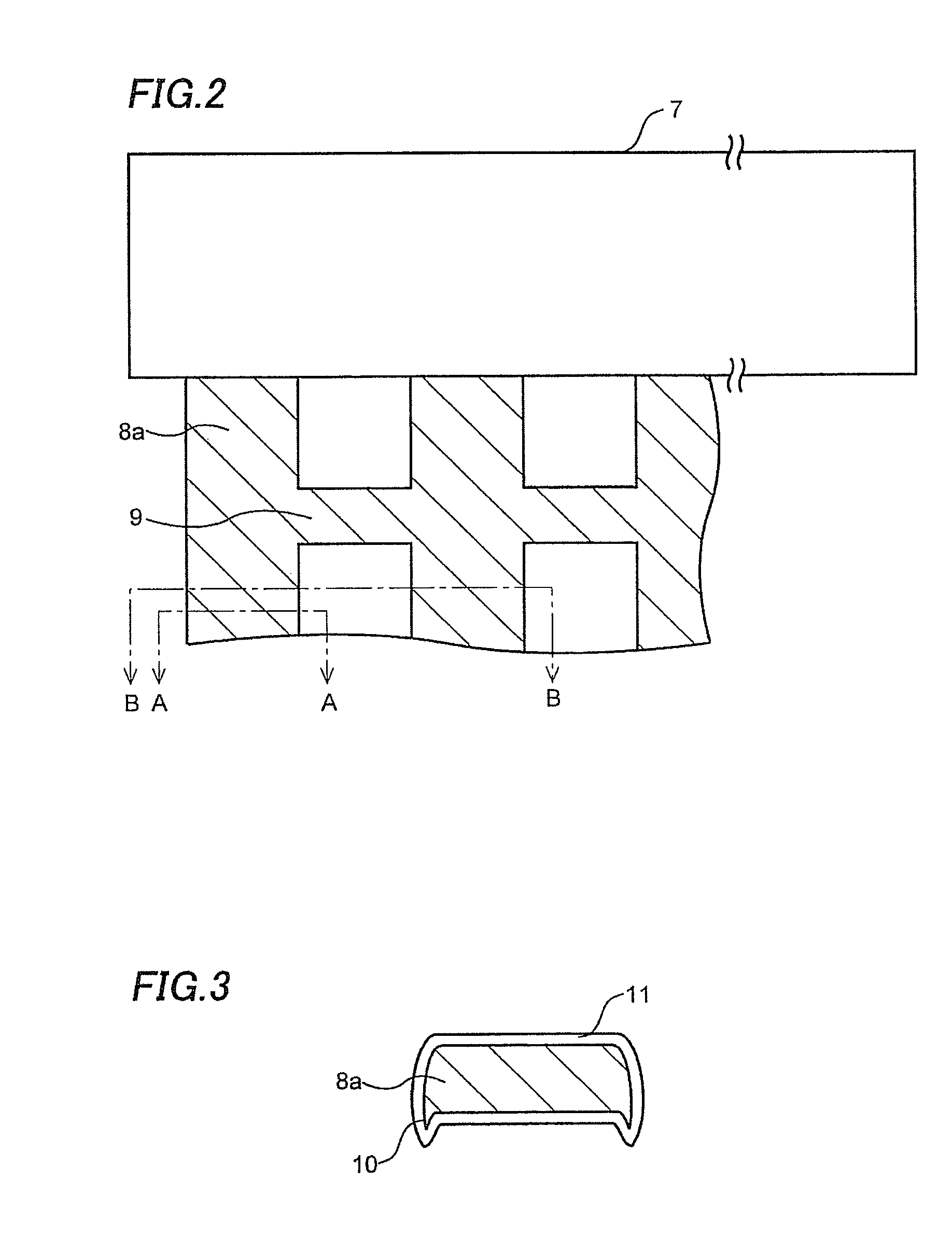
[0030]the invention relates to the prevention of a problem that a solder plating layer 11 attached to a small lead burr 10 of a lead frame 1 formed by presswork peels off the lead burr 10 when a tie bar 9 is cut and forms a mustache-like solder burr 12 to cause short circuit between outer leads 8a and so on. The description will be given below referring to FIGS. 1 to 11.

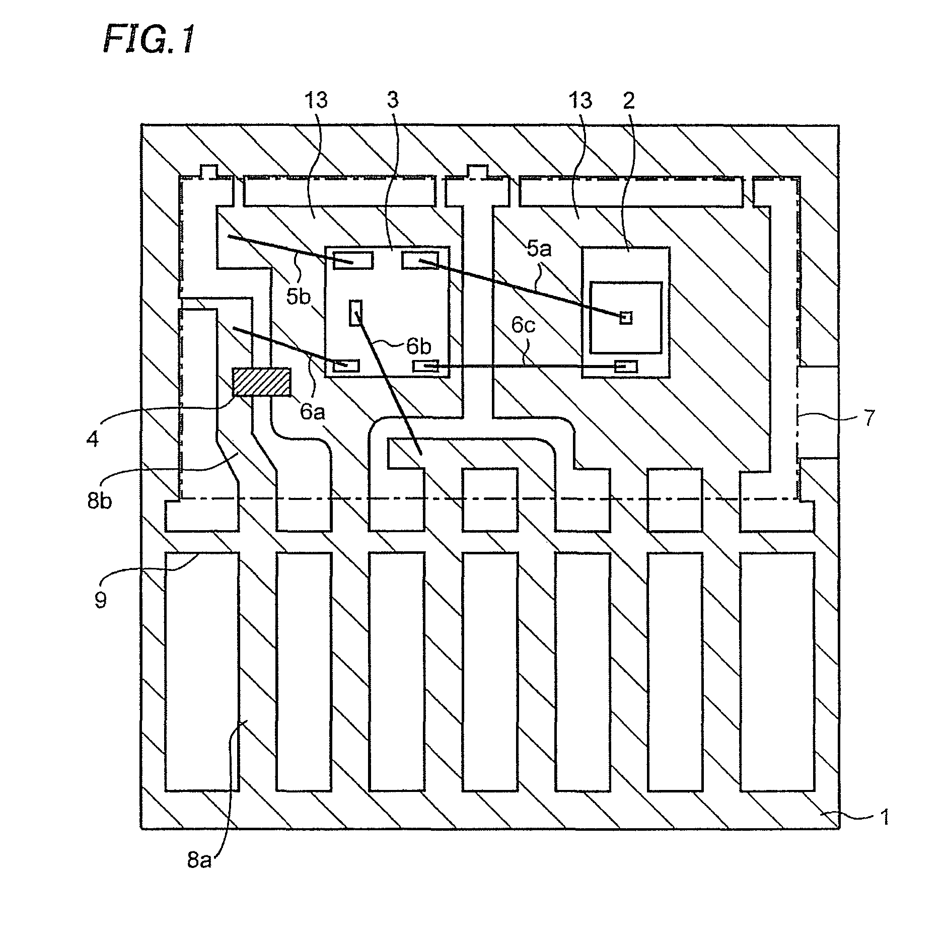
[0031]Although there are some types of lead frame 1 for use in which a plurality of same patterns is arrayed in a single row, in two rows or in three rows, the description will be given by showing one of the patterns in detail since this embodiment is understood by describing one pattern. The description will be given using a simple package of an SIP (Single In-line Package) type as a package, provided with a series of outer leads and tie bars.

[0032]First, a Cu member is pressed and formed and Ni or the like is plated on the surface thereof to provide a lead frame 1. Then, as shown in FIG. 1, a semiconductor die 2, a...

third embodiment

[0067]The third embodiment is described using SIP of six terminals as an example, the invention is also applicable to a resin sealing type electronic device of other type. Furthermore, the die capacitor 17 is an example of an electronic component, and an electronic component of any other type may be used as long as it is bonded to a lead.

[0068]By the method of manufacturing the resin sealing type semiconductor device of the invention, the resin sealing type semiconductor device with high reliability is manufactured by preventing the mustache-like solder burr 12 caused by the lead burr 10 formed on the lead frame 1 by presswork.

[0069]Furthermore, the resin sealing type electronic device of the invention prevents a failure in welding the outer lead to an external electrode, and secures the large connection area of the electronic component to the lead to prevent a connection failure therebetween.


PUM


Abstract

The invention provides a resin sealing type electronic device having high reliability by eliminating a solder burr formed when a tie bar is cut. The invention also prevents a welding failure between a lead of the resin sealing type electronic device and an external electrode, and provides a large area for bonding an electronic component to the lead to prevent a connection failure. In the method of manufacturing the resin sealing type semiconductor device of the invention, in a case that a tie bar is cut after a semiconductor die and so on are mounted on a lead frame and these are resin-sealed, the cutting of the tie bar is performed from the side of the lead frame where a lead burr is formed by presswork. Furthermore, in the resin sealing type electronic device of the invention, a die capacitor is bonded to burr formation surfaces of a lead and an island using conductive paste. Since the burr formation surface has a larger surface area than a rounded surface, a large bonding area is obtained. A welding surface of the lead to a control electrode is the rounded surface that is opposite to the burr formation surface.

Description

CROSS-REFERENCE OF THE INVENTION[0001]This application claims priority from Japanese Patent Application Nos. 2008-219943, 2008-220979, and 2009-108811, the content of which is incorporated herein by reference in its entirety.BACKGROUND OF THE INVENTION[0002]1. Field of the Invention[0003]The invention relates to a resin sealing type semiconductor device in which an electronic component and so on are resin-sealed and a method of manufacturing the same. The invention also relates to a resin sealing type electronic device in which an electronic component and so on are resin-sealed.[0004]2. Description of the Related Art[0005]A resin sealing type semiconductor device in which a semiconductor die is sealed in a resin package and a resin sealing type electronic device in which an electronic component and so on are sealed in a resin package have been conventionally known. These resin sealing type semiconductor devices and so on are completed by providing a lead frame, die-bonding various s...

Claims


Application Information

Patent Timeline
Patent Type & Authority Patents(United States)
IPC IPC(8): H01L23/495
CPCH01L21/4842H01L21/565H01L23/49548H01L23/49562H01L23/49575H01L23/49582H01L23/49589H01L24/06H01L24/49H01L24/45H01L24/85H01L2224/05553H01L2224/05599H01L2224/0603H01L2224/29339H01L2224/45124H01L2224/45144H01L2224/48091H01L2224/48137H01L2224/48247H01L2224/4903H01L2224/49051H01L2224/49171H01L2224/85201H01L2224/85399H01L2924/01004H01L2924/01005H01L2924/01013H01L2924/01015H01L2924/01027H01L2924/01028H01L2924/01029H01L2924/01033H01L2924/01047H01L2924/0105H01L2924/01078H01L2924/01079H01L2924/01082H01L2924/014H01L2924/13055H01L2924/13091H01L2924/14H01L2924/19041H01L2924/19105H01L24/48H01L2924/00014H01L2924/01006H01L2224/48599H01L2224/48699H01L2924/1305H01L2924/00
Inventor SASAKI, TAKESHISHINDO, MASAHIRO
Owner SEMICON COMPONENTS IND LLC
Why Eureka
Try Eureka