Protecting circuit and control circuit for reducing leakage current

a technology of leakage current and protection circuit, applied in the direction of voltage/current interference elimination, circuit arrangement, reliability increasing modifications, etc., can solve the problem of reducing the efficiency of complementary metal-oxide-semiconductor, gidl is serious, and the gidl will become more serious, so as to reduce the voltage difference and reduce the gidl

Active Publication Date: 2013-08-06
WINBOND ELECTRONICS CORP
View PDF8 Cites 0 Cited by
  • Summary
  • Abstract
  • Description
  • Claims
  • Application Information

AI Technical Summary

Benefits of technology

[0005]For solving the GIDL problem, the invention provides a protecting circuit and a control circuit that can reduce the voltage difference between a gate and a drain so as to reduce GIDL.

Problems solved by technology

Gate induced drain leakage (GIDL) is a serious problem for complementary metal-oxide-semiconductors (CMOS).
If the voltage difference between a gate and a drain of a transistor becomes higher, GIDL will become more serious.
That is, the complementary metal-oxide-semiconductor will consume more electrical power in vain.

Method used


Image

  • Protecting circuit and control circuit for reducing leakage current
  • Protecting circuit and control circuit for reducing leakage current
  • Protecting circuit and control circuit for reducing leakage current

Examples


Embodiment Construction

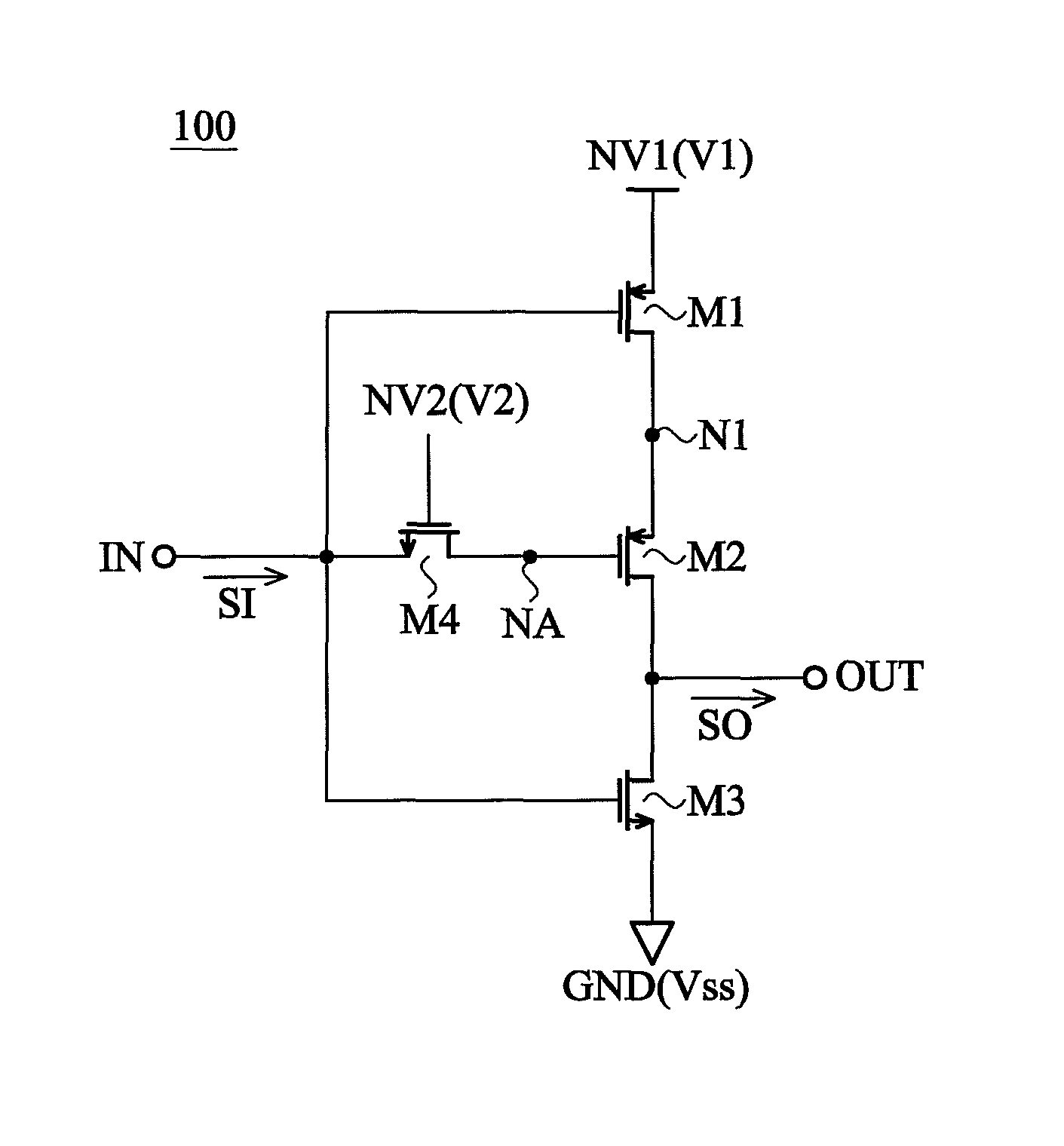
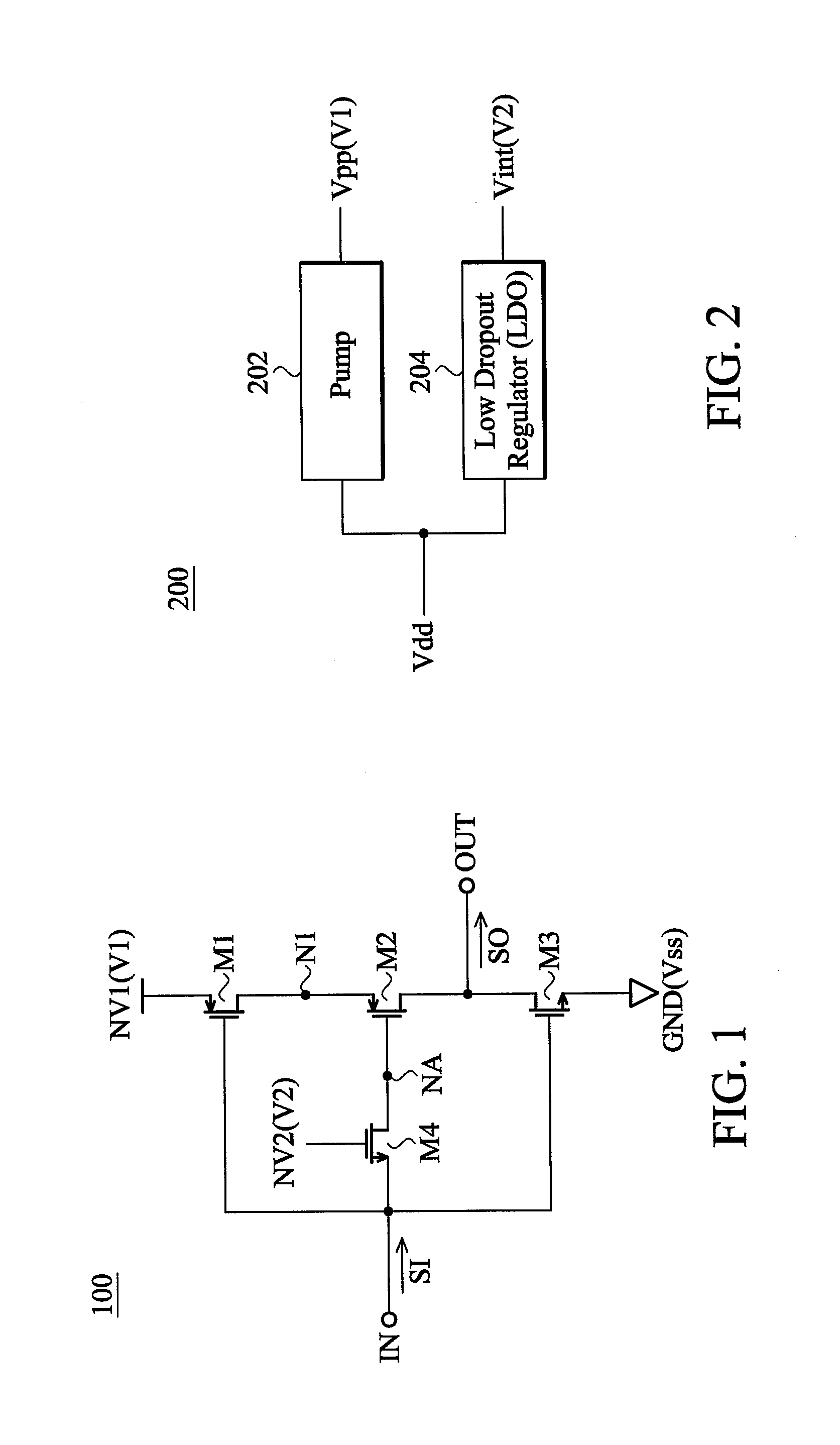
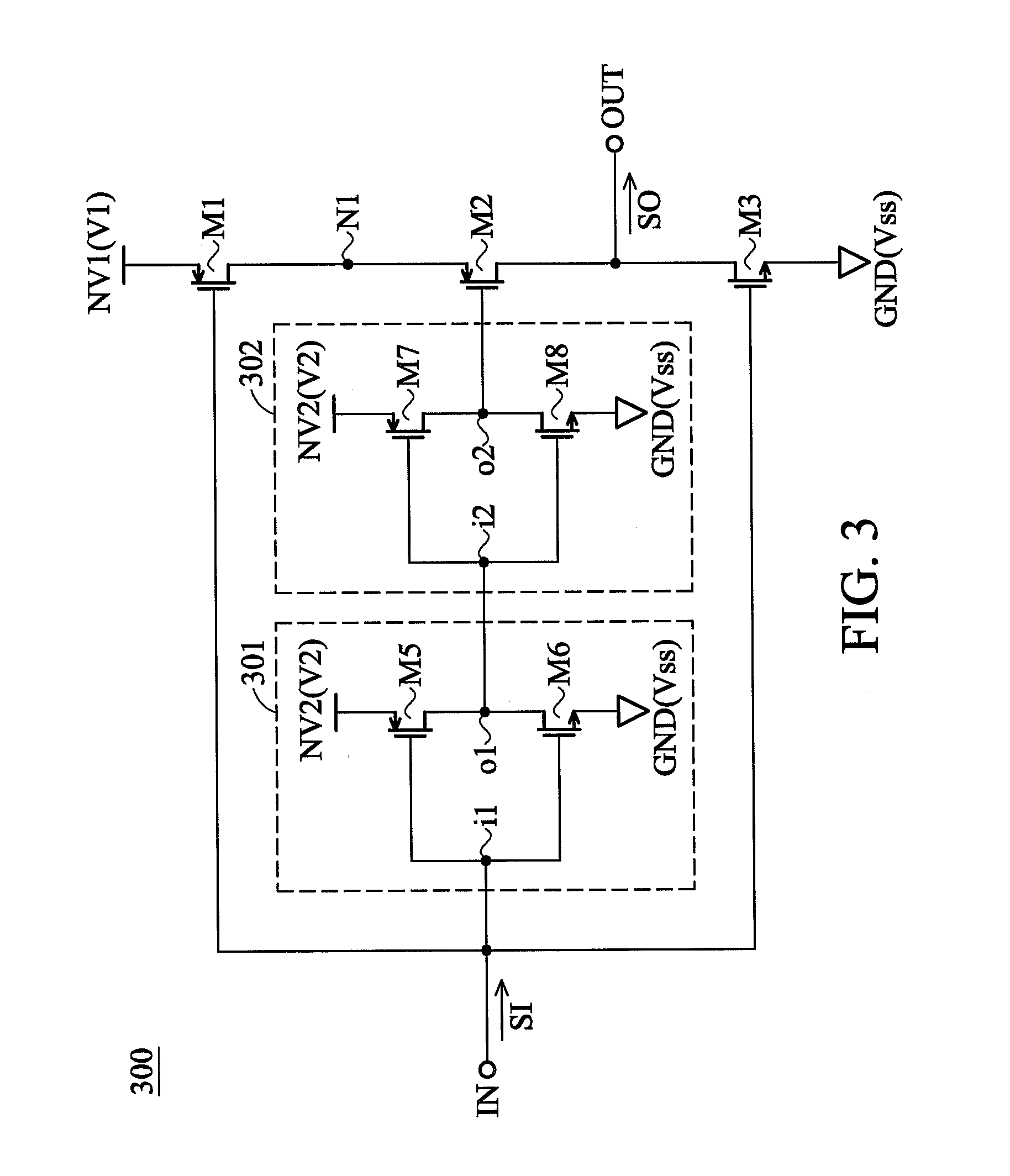
[0014]FIG. 1 is a diagram for illustrating a protecting circuit 100 according to an embodiment of the invention. As shown in FIG. 1, the protecting circuit 100 comprises PMOS transistors (P-channel Metal-Oxide-Semiconductor Field-Effect Transistor) M1, M2, and NMOS transistors (N-channel Metal-Oxide-Semiconductor Field-Effect Transistor) M3, M4. A ground node GND is configured to provide a ground voltage Vss. A first voltage node NV1 is configured to provide a first voltage V1, and a second voltage node NV2 is configured to provide a second voltage V2, wherein each of the first and second voltages V1, V2 is higher than the ground voltage Vss.

[0015]FIG. 2 is a diagram for illustrating a conversion circuit 200 according to an embodiment of the invention. As shown in FIG. 2, an external voltage Vdd (i.e., work voltage Vdd) of the protecting circuit is converted into a pump voltage Vpp through a pump 202 (i.e., a step-up circuit), and the external voltage Vdd is converted into an intern...


PUM


Abstract

A protecting circuit for reducing leakage currents comprises a first PMOS transistor (P-channel Metal-Oxide-Semiconductor Field-Effect Transistor), a second PMOS transistor, a first NMOS transistor (N-channel Metal-Oxide-Semiconductor Field-Effect Transistor), and a second NMOS transistor. The first PMOS transistor is coupled between a first voltage node and a node, and comprises a first gate coupled an input node. The second PMOS transistor is coupled between the node and an output node. The first NMOS transistor is coupled between the output node and a ground node, and comprises a third gate coupled to the input node. The second NMOS transistor is coupled between the input node and a second gate of the second PMOS transistor, and comprises a fourth gate coupled to a second voltage node.

Description

BACKGROUND OF THE INVENTION[0001]1. Field of the Invention[0002]The disclosure generally relates to a protecting circuit, and more particularly, relates to a protecting circuit for reducing leakage currents[0003]2. Description of the Related Art[0004]Gate induced drain leakage (GIDL) is a serious problem for complementary metal-oxide-semiconductors (CMOS). GIDL is a current in an off-state. If the voltage difference between a gate and a drain of a transistor becomes higher, GIDL will become more serious. That is, the complementary metal-oxide-semiconductor will consume more electrical power in vain.BRIEF SUMMARY OF THE INVENTION[0005]For solving the GIDL problem, the invention provides a protecting circuit and a control circuit that can reduce the voltage difference between a gate and a drain so as to reduce GIDL.[0006]In one exemplary embodiment, the disclosure is directed to a protecting circuit for reducing leakage currents, comprising: a first PMOS transistor (P-channel Metal-Ox...

Claims


Application Information

Patent Timeline
Patent Type & Authority Patents(United States)
IPC IPC(8): H02H7/00
CPCH03K19/00361H01L27/0285
Inventor LIN, CHE-MIN
Owner WINBOND ELECTRONICS CORP
Why Eureka
Try Eureka