Encapsulating package, printed circuit board, electronic device and method for manufacturing encapsulating package

a technology of encapsulating package and printed circuit board, which is applied in the field of encapsulating package, can solve the problems of reduced saturated, and inability to adsorb gas no more, and achieve the effects of reducing the performance of electronic devices, and reducing the sensitivity of output signals

Active Publication Date: 2013-09-03
GK BRIDGE 1
View PDF21 Cites 13 Cited by
  • Summary
  • Abstract
  • Description
  • Claims
  • Application Information

AI Technical Summary

Benefits of technology

[0023]1) For example, to describe using FIG. 43, in the case of performing a process of sealing the vacuum sealing hole (sealing hole) 119 using the sealing material 120, the entire infrared ray detecting package or the infrared optical component (detection target selecting material) in the vicinity of the sealing material 120 will also have to be heated, and therefore the melting point of the sealing material 120 needs to be considerably lower than the melting point of the fixing material 118 which bonds the infrared optical component (detection target selecting material) 117 and the lid (container main body) 115. However, considering the points including reliability and manufacturing process, it is realistically difficult to select a fixing material 118 and a sealing material 120 having a considerable difference in the melting point therebetween (that is to say, manufacturing is difficult), and also the level of freedom allowed in the structure design is reduced.
[0024]2) Moreover, since the method is such that having performed vacuuming from the vacuum sealing hole (sealing hole) 119 in the vacuum atmosphere, the sealing material 120 is placed in the vacuum sealing hole (sealing hole) 119 and is then melted, it is difficult to handle the sealing material 120 in the vacuum atmosphere. There is a possible method in which, for example, a mechanism such as robot-handling mechanism is installed inside a vacuum apparatus. However, the cost of apparatus manufacturing becomes high as the level of quality and performance of each component thereof need to be high in order to realize a high level of vacuum, the cost of manufacturing the robot-handling mechanism itself is high in the first place, and further, the size of the entire apparatus is made large by providing a transporting mechanism. As a result, it leads to high manufacturing cost for the vacuum apparatus for manufacturing a vacuum encapsulating package.
[0032]The present invention takes into consideration the above circumstances, and an object thereof is to provide an airtight encapsulating package, a vacuum encapsulating package, a printed circuit board having these mounted thereon, an electronic device, and a method for manufacturing an encapsulating package, in which a through hole can be quickly and easily blocked, no expensive vacuum apparatus (with a movable machine component provided therein, or with a robot-handling mechanism or the like provided therein) is used, superior productivity can be achieved, there is provided a function of preventing a reduction in the level of vacuum even on a long term basis, and the manufacturing cost thereof can be reduced.Means for Solving the Problem
[0059]Moreover, the present invention includes: a mounting step of mounting a getter material capable of adsorbing gas molecules, at a position inside the package main body section where it is contactable with a laser beam irradiated through the through hole; a vacuuming step of vacuuming inside of a vacuum chamber where the first main body section and the second main body section bonded in the bonding step are installed, to thereby vacuum inside the hollow section via the through hole; and a heating step of irradiating a laser beam through the through hole to thereby heat the getter material.

Problems solved by technology

As a result, there is a problem in that the performance of the electronic device is reduced (in an infrared ray sensor for example, the sensitivity of output signals is reduced).
However, if it is left in the atmosphere, gas molecules become adsorbed on the surface thereof, and consequently it becomes saturated and unable to adsorb gas no more.

Method used


Image

  • Encapsulating package, printed circuit board, electronic device and method for manufacturing encapsulating package
  • Encapsulating package, printed circuit board, electronic device and method for manufacturing encapsulating package
  • Encapsulating package, printed circuit board, electronic device and method for manufacturing encapsulating package

Examples


exemplary embodiment 1

(Exemplary Embodiment 1)

[0140]Hereunder, an encapsulating package in a first exemplary embodiment of the present invention is described, with reference to drawings.

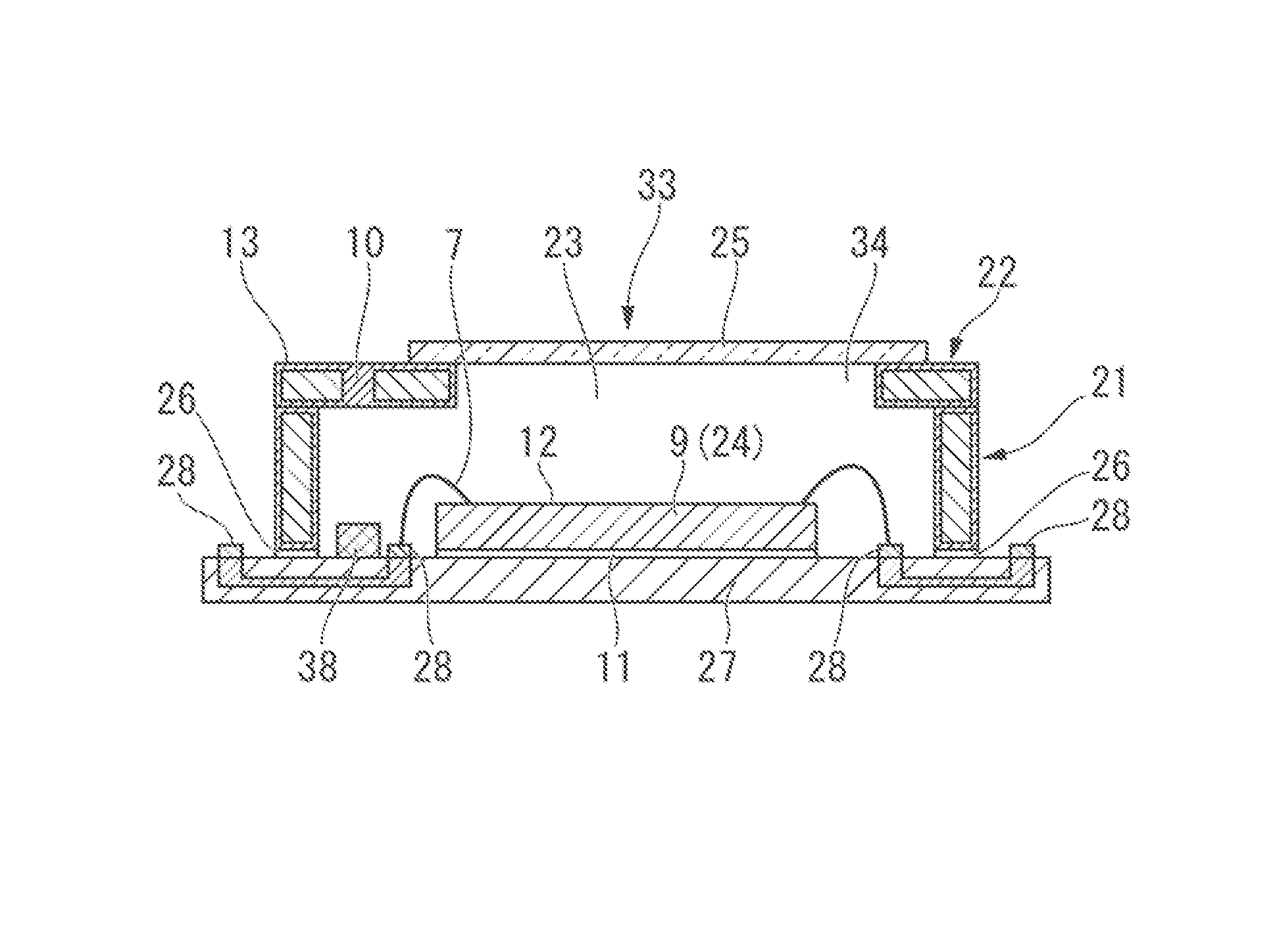
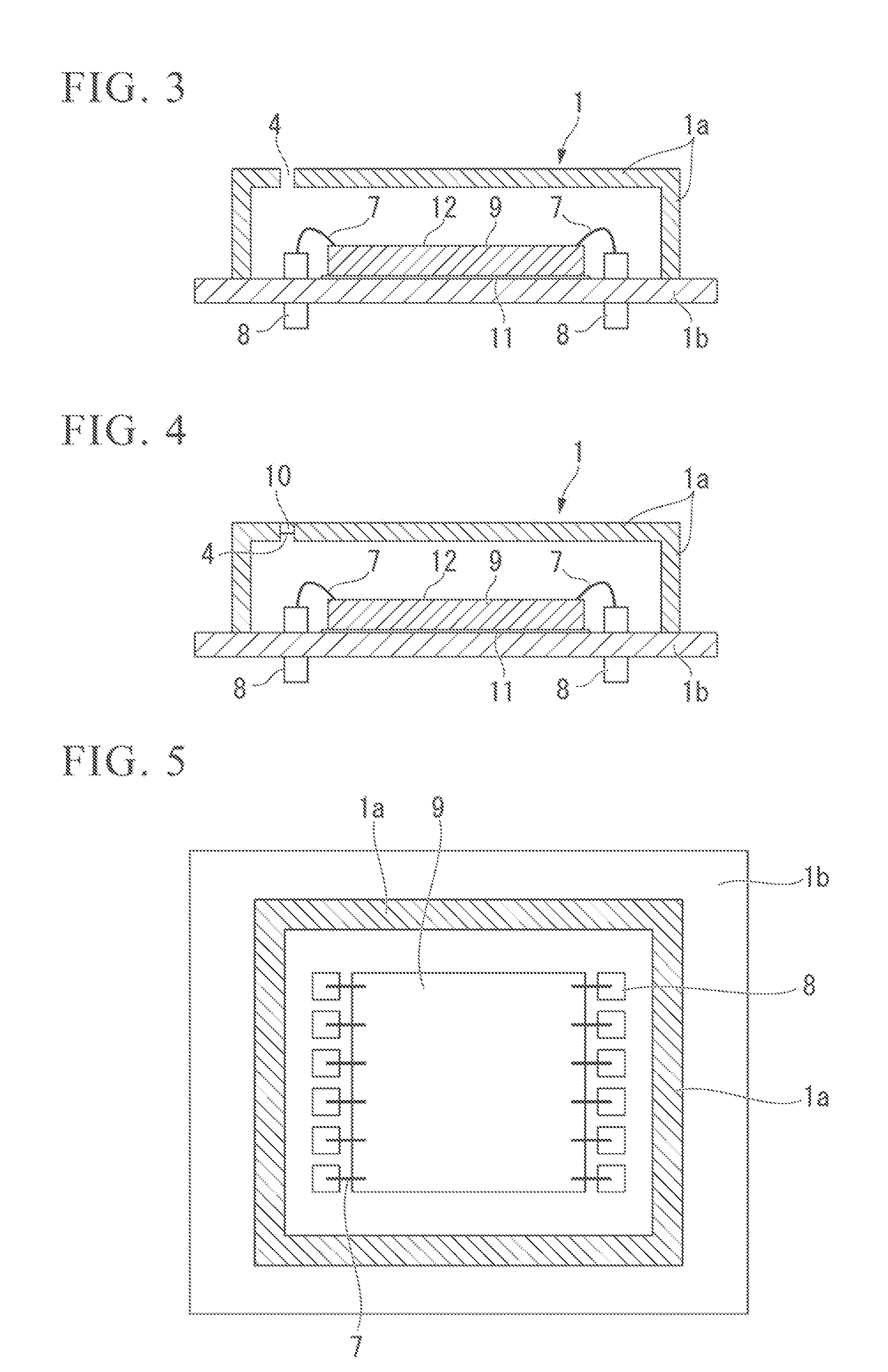
[0141]FIG. 4 and FIG. 5 show the encapsulating package as the first exemplary embodiment of the present invention.

[0142]FIG. 3 shows a state prior to blocking a through hole 4.

[0143]The encapsulating package includes a structure (package main body section) serving as a package main body. This package main body section 1 includes a structure (first main body section) 1b formed in a rectangular plate shape, and a structure (second main body section) 1a bonded with this structure 1b.

[0144]The structure 1a is formed in a hollow rectangular box shape, and one surface of side surface sections thereof is open. That is to say, the structure 1a is a sectionally channel-shaped surface when seen from a side. Further, the structure 1a and the structure 1b are bonded so as to cover the open portion of the structure 1a.

[0145]There ar...

exemplary embodiment 2

(Exemplary Embodiment 2)

[0172]Next, a second exemplary embodiment of the present invention is described.

[0173]FIG. 15 and FIG. 16 show the second exemplary embodiment of the present invention.

[0174]In FIG. 15 and FIG. 16, the same reference symbols are given to portions the same as constituents described in FIG. 1 to FIG. 4, and descriptions thereof are omitted.

[0175]The basic configuration of this embodiment is the same as that of the first exemplary embodiment described above, and points of difference therebetween are mainly described here.

[0176]FIG. 16 is a cross-sectional view showing an encapsulating package in the second exemplary embodiment of the present invention.

[0177]FIG. 15 is a cross-sectional view showing a state of a through hole 4 in FIG. 16 prior to being blocked.

[0178]In the first exemplary embodiment of the present invention shown in FIG. 4 and FIG. 5, there is illustrated the example of the electronic device 9 being electrically connected to the pin (output termi...

exemplary embodiment 3

(Exemplary Embodiment 3)

[0181]Next, a third exemplary embodiment of the present invention is described.

[0182]FIG. 17 and FIG. 18 show the third exemplary embodiment of the present invention.

[0183]In FIG. 17 and FIG. 18, the same reference symbols are given to portions the same as constituents described in FIG. 1 to FIG. 16, and descriptions thereof are omitted.

[0184]The basic configuration of this embodiment is the same as that of the first exemplary embodiment described above, and points of difference therebetween are mainly described here.

[0185]FIG. 18 is a cross-sectional view showing an encapsulating package in the third exemplary embodiment of the present invention.

[0186]FIG. 17 is a cross-sectional view showing a state of a through hole 4 in FIG. 18 prior to being blocked.

[0187]The first and second exemplary embodiments illustrates the examples of the electronic device 9 being mounted on the structure 1b via the bonding material 11. On the other hand, the encapsulating package...


PUM

PropertyMeasurementUnit
thicknessaaaaaaaaaa
thicknessaaaaaaaaaa
melting pointaaaaaaaaaa

Abstract

The present invention is: a package main body section having a hollow section; and an electronic device provided in the hollow section in the package main body section, in the package main body section, there being formed a through hole, through which the hollow section communicates with outside of the package main body section, and in the through hole, there being provided a sealing section in which a vicinity of the through hole is partly heated and a constituent material of the package main body section is melted to thereby block the through hole.

Description

[0001]This application is the National Phase of PCT / JP2009 / 051325, filed Jan. 28, 2009, which is based upon and claims the benefit of priority from Japanese Patent Application No. 2008-192342, filed on Jul. 25, 2008, the content of which is incorporated herein in its entirety by reference.TECHNICAL FIELD[0002]The present invention relates to an encapsulating package having an electronic device encapsulated therein, and a manufacturing method thereof.BACKGROUND ART[0003]In recent years, for a package or a device having an electronic device such as an infrared ray sensor, gyro sensor (angular velocity sensor), temperature sensor, pressure sensor, and acceleration sensor vacuum-encapsulated therein, there has been a demand for miniaturization, technological advances in performance, and cost reductions. In particular, for a package or a device having an infrared ray sensor, which is used in a surveillance camera for night-time security or is used in thermography for calculating and disp...

Claims


Application Information

Patent Timeline
Patent Type & Authority Patents(United States)
IPC IPC(8): H01L23/12
CPCH01L31/0203H01L21/54H01L23/055G01J5/04H05K3/30G01J5/045H01L23/10H01L23/26H01L2224/73265H01L2924/10253H01L2924/01079H01L2224/32225H01L2924/16152H01L2924/3025H01L2924/15192H01L2224/4823Y10T29/49146H01L2224/92247H01L2924/09701H01L2924/15311H01L2924/16151H01L2224/48227H01L2224/48091H01L2924/00014H01L2924/00H01L2924/00012H01L24/73
Inventor YAMAZAKI, TAKAOSANO, MASAHIKOKURASHINA, SEIJISOGAWA, YOSHIMICHI
Owner GK BRIDGE 1
Why Eureka
Try Eureka