Encapsulating package, printed circuit board, electronic device and method for manufacturing encapsulating package

a technology of printed circuit boards and encapsulating packages, which is applied in the direction of optical radiation measurement, electrical apparatus casings/cabinets/drawers, instruments, etc., can solve the problems of reduced sensitivity of output signals, saturated, and inability to adsorb gas no more, and reduce the performance of electronic devices

Active Publication Date: 2011-05-19
GK BRIDGE 1
View PDF8 Cites 69 Cited by
  • Summary
  • Abstract
  • Description
  • Claims
  • Application Information

AI Technical Summary

Benefits of technology

[0059]Moreover, the present invention includes: a mounting step of mounting a getter material capable of adsorbing gas molecules, at a position inside the package main body section where it is contactable with a laser beam irradiated through the through hole; a vacuuming step of vacuuming inside of

Problems solved by technology

As a result, there is a problem in that the performance of the electronic device is reduced (in an infrared ray sensor for example, the sensitivity of output signals is red

Method used


Image

  • Encapsulating package, printed circuit board, electronic device and method for manufacturing encapsulating package
  • Encapsulating package, printed circuit board, electronic device and method for manufacturing encapsulating package
  • Encapsulating package, printed circuit board, electronic device and method for manufacturing encapsulating package

Examples


exemplary embodiment 1

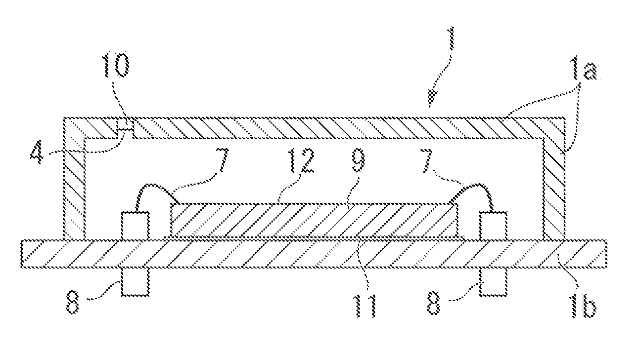
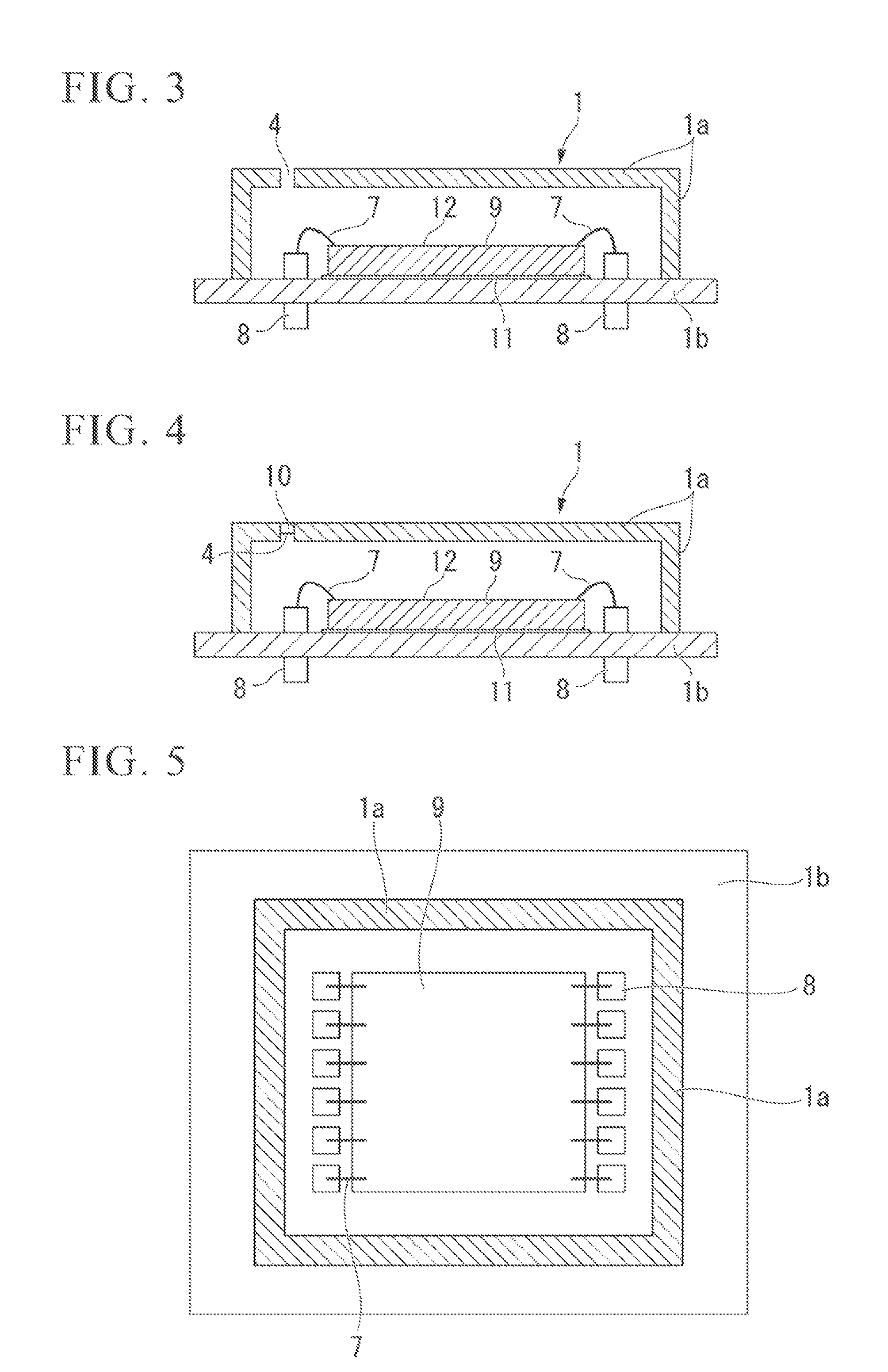
[0140]Hereunder, an encapsulating package in a first exemplary embodiment of the present invention is described, with reference to drawings.

[0141]FIG. 4 and FIG. 5 show the encapsulating package as the first exemplary embodiment of the present invention.

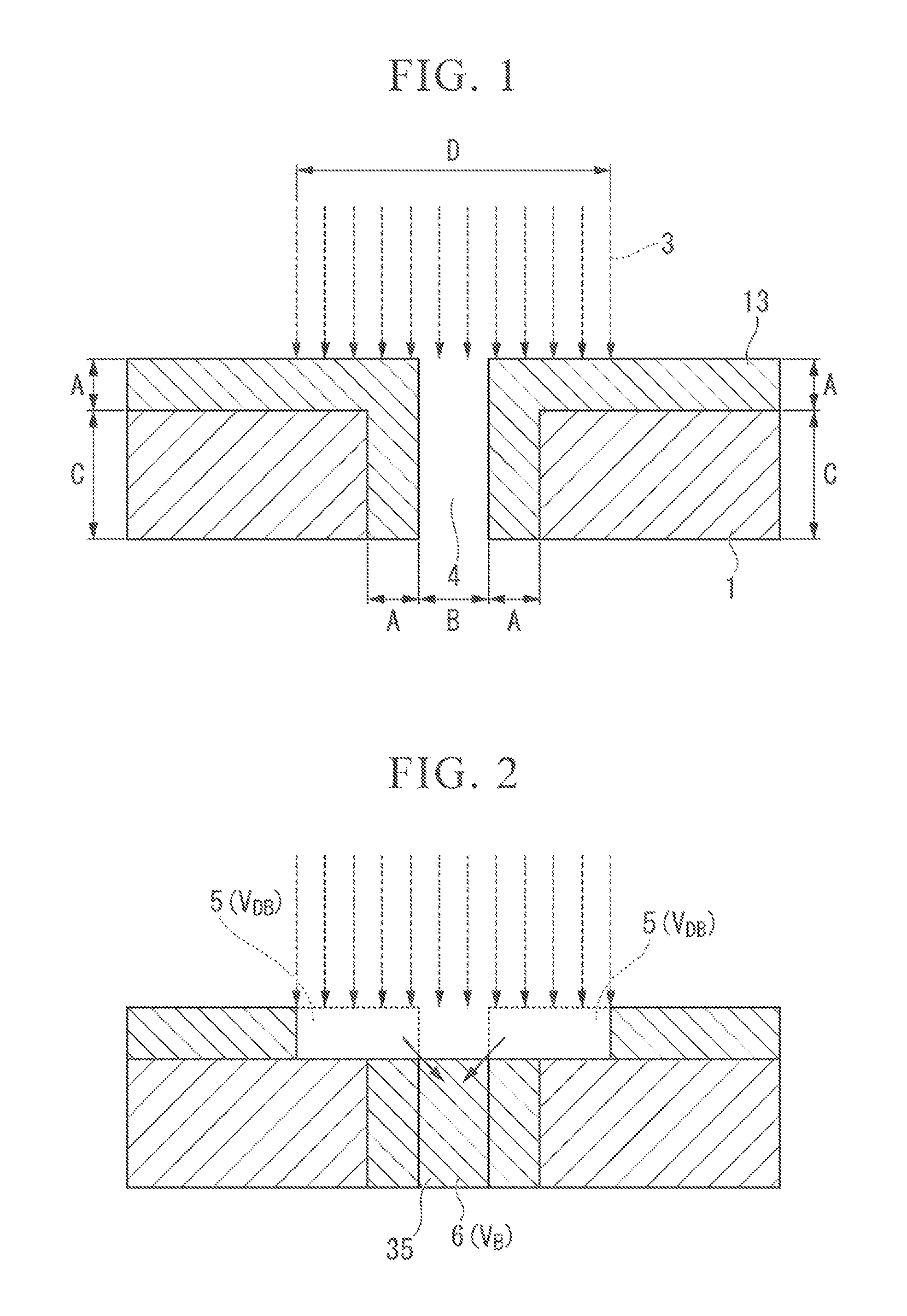
[0142]FIG. 3 shows a state prior to blocking a through hole 4.

[0143]The encapsulating package includes a structure (package main body section) serving as a package main body. This package main body section 1 includes a structure (first main body section) 1b formed in a rectangular plate shape, and a structure (second main body section) 1a bonded with this structure 1b.

[0144]The structure 1a is formed in a hollow rectangular box shape, and one surface of side surface sections thereof is open. That is to say, the structure 1a is a sectionally channel-shaped surface when seen from a side. Further, the structure 1a and the structure 1b are bonded so as to cover the open portion of the structure 1a.

[0145]There are no particular limitati...

exemplary embodiment 2

[0172]Next, a second exemplary embodiment of the present invention is described.

[0173]FIG. 15 and FIG. 16 show the second exemplary embodiment of the present invention.

[0174]In FIG. 15 and FIG. 16, the same reference symbols are given to portions the same as constituents described in FIG. 1 to FIG. 4, and descriptions thereof are omitted.

[0175]The basic configuration of this embodiment is the same as that of the first exemplary embodiment described above, and points of difference therebetween are mainly described here.

[0176]FIG. 16 is a cross-sectional view showing an encapsulating package in the second exemplary embodiment of the present invention.

[0177]FIG. 15 is a cross-sectional view showing a state of a through hole 4 in FIG. 16 prior to being blocked.

[0178]In the first exemplary embodiment of the present invention shown in FIG. 4 and FIG. 5, there is illustrated the example of the electronic device 9 being electrically connected to the pin (output terminal) 8 by the wire line ...

exemplary embodiment 3

[0181]Next, a third exemplary embodiment of the present invention is described.

[0182]FIG. 17 and FIG. 18 show the third exemplary embodiment of the present invention.

[0183]In FIG. 17 and FIG. 18, the same reference symbols are given to portions the same as constituents described in FIG. 1 to FIG. 16, and descriptions thereof are omitted.

[0184]The basic configuration of this embodiment is the same as that of the first exemplary embodiment described above, and points of difference therebetween are mainly described here.

[0185]FIG. 18 is a cross-sectional view showing an encapsulating package in the third exemplary embodiment of the present invention.

[0186]FIG. 17 is a cross-sectional view showing a state of a through hole 4 in FIG. 18 prior to being blocked.

[0187]The first and second exemplary embodiments illustrates the examples of the electronic device 9 being mounted on the structure 1b via the bonding material 11. On the other hand, the encapsulating package in the third exemplary ...


PUM

PropertyMeasurementUnit
Thicknessaaaaaaaaaa
Diameteraaaaaaaaaa
Widthaaaaaaaaaa

Abstract

The present invention is: a package main body section having a hollow section; and an electronic device provided in the hollow section in the package main body section, in the package main body section, there being formed a through hole, through which the hollow section communicates with outside of the package main body section, and in the through hole, there being provided a sealing section in which a vicinity of the through hole is partly heated and a constituent material of the package main body section is melted to thereby block the through hole.

Description

[0001]This application is based upon and claims the benefit of priority from Japanese Patent Application No. 2008-192342, filed on Jul. 25, 2008, the content of which is incorporated herein in its entirety by reference.TECHNICAL FIELD[0002]The present invention relates to an encapsulating package having an electronic device encapsulated therein, and a manufacturing method thereof.BACKGROUND ART[0003]In recent years, for a package or a device having an electronic device such as an infrared ray sensor, gyro sensor (angular velocity sensor), temperature sensor, pressure sensor, and acceleration sensor vacuum-encapsulated therein, there has been a demand for miniaturization, technological advances in performance, and cost reductions. In particular, for a package or a device having an infrared ray sensor, which is used in a surveillance camera for night-time security or is used in thermography for calculating and displaying temperature distribution, mounted therein, the inside thereof ne...

Claims


Application Information

Patent Timeline
IPC IPC(8): G01J5/10H01L23/28H05K5/00H01L23/48H05K3/30
CPCH01L2224/73265H01L2924/10253H01L2924/01079H01L2224/32225H01L2924/16152H01L2924/3025H01L2924/15192H01L31/0203H01L21/54H01L2224/4823H01L23/055Y10T29/49146H01L2224/92247G01J5/04H01L2924/09701H05K3/30G01J5/045H01L23/10H01L2924/15311H01L2924/16151H01L2224/48227H01L23/26H01L2224/48091H01L2924/00014H01L2924/00H01L2924/00012H01L24/73
Inventor YAMAZAKI, TAKAOSANO, MASAHIKOKURASHINA, SEIJISOGAWA, YOSHIMICHI
Owner GK BRIDGE 1
Why Eureka
Try Eureka