
Method for manufacturing a three dimensional circuit board

a three-dimensional circuit board and manufacturing method technology, applied in the direction of printed circuit aspects, printed element electric connection formation, conductive pattern formation, etc., can solve the problems of either difficult or impossible deposit of electroless plating, and achieve the effect of preventing the damage of the molding die, preventing the splash of solder, and reliable deposit of plating

Inactive Publication Date: 2013-09-10
SANKYO KASEI CO LTD
View PDF16 Cites 0 Cited by
  • Summary
  • Abstract
  • Description
  • Claims
  • Application Information

AI Technical Summary

Benefits of technology

The present invention helps prevent damage to a molding die and ensures a reliable deposit in plating. It allows for smaller circuit patterns on a circuit board, prevents solder splash and short-circuits, and enhances the reliability of solid or three-dimensional circuits. The blind through hole also eliminates the need for cleaning flux and prevents the outflow of solder when mounting circuits.

Problems solved by technology

Namely, if the aspect ratio falls within 5:1, electroless plating can deposit, however, if the aspect ratio exceeds 5:1, deposit by electroless plating is either difficult or impossible.

Method used


Image

  • Method for manufacturing a three dimensional circuit board
  • Method for manufacturing a three dimensional circuit board
  • Method for manufacturing a three dimensional circuit board

Examples


Embodiment Construction

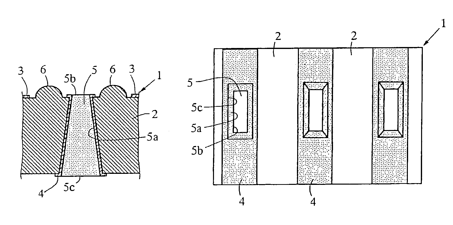
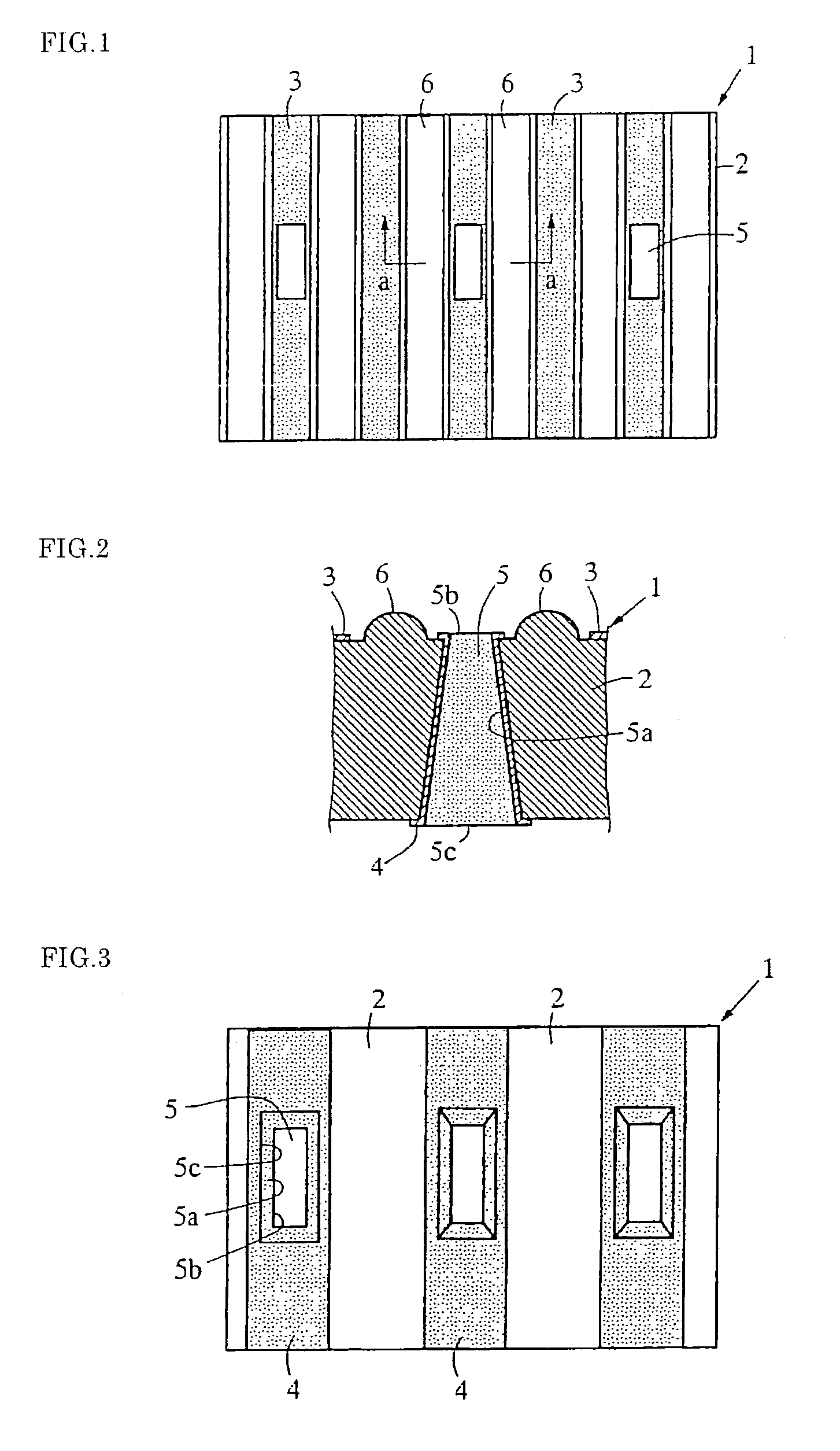
[0034]A structure of a solid or three dimensional circuit board 1 according to the present invention will be described below with reference to FIGS. 1 to 3. A circuit board 2 is made of a primary molded article of an insulating material and is plated. One side of the circuit board 2 is provided with a pre-determined circuit patterns 3, 3, . . . of a conductive material as shown in FIG. 1. The other side of the circuit board 2 is provided with a pre-determined circuit patterns 4, 4, . . . of a conductive material as shown in FIG. 3. Through hole 5, 5, . . . of conductive layer 5a are formed on the circuit board 2, which electrically connect the circuit patterns 3, 3, . . . and 4, 4, . . . as shown in FIG. 2.

[0035]The through hole 5 is shaped such that its width in the circuit-extended direction is larger than that in the circuit-pattern 3, 3-lined direction. The circuit-pattern 3, 3-lined direction means that a direction along which the circuit patterns 3, 3, . . . are lined up. For ...


PUM

PropertyMeasurementUnit
diameteraaaaaaaaaa
aspect ratioaaaaaaaaaa

Abstract

A molding pin for a metal die is prevented from breaking, solder is surely deposited, and thus, a circuit pitch can be reduced to the limit. On the front plane of a circuit board, prescribed circuit patterns made of a conductive material are formed, and on the rear plane, prescribed circuit patterns are also formed. On the circuit board, a through hole is formed to carry electricity between the circuit patterns on both planes. The inner shape of the through hole is narrow in a direction between the adjacent circuit patterns and wide in a circuit extending direction.

Description

TECHNICAL FIELD[0001]The present invention relates to a method for manufacturing a solid or three-dimensional circuit board.BACKGROUND ART[0002]In recent years, demands for making much narrower intervals or pitches between circuit patterns on a circuit board increase to make electronic devices much smaller and to save resources and energy for their manufacturing. Accordingly, circuit patterns are formed on the both sides of a circuit board, which are electrically connected by a through hole of a conductive layer. Although the through hole is conventionally formed by drilling, recently it is formed during the injection-molding process for the circuit board itself (Patent Documents 1, 2, and 3).[0003]Patent Document 1: JP unexamined patent application publication No. 61-239694[0004]Patent Document 2: JP unexamined patent application publication No. 63-128181[0005]Patent Document 3: U.S. Pat. No. 4,424,095[0006]Structure of a conventional solid or three-dimensional circuit board 11 wil...

Claims


Application Information

Patent Timeline
Patent Type & Authority Patents(United States)
IPC IPC(8): H05K3/42H05K1/00H05K1/02H05K1/11
CPCH05K1/115H05K1/0284H05K3/42H05K2201/09045H05K2201/09118H05K2201/09236Y10T29/49155H05K2201/09827H05K2201/09854Y10T29/49176Y10T29/49165Y10T29/4916Y10T29/49158H05K2201/0959G01R31/28
Inventor YUMOTO, TETSUO
Owner SANKYO KASEI CO LTD
Learn More