Method for positioning chips during the production of a reconstituted wafer

Active Publication Date: 2013-10-01
3D PLUS
View PDF48 Cites 3 Cited by
  • Summary
  • Abstract
  • Description
  • Claims
  • Application Information

AI Technical Summary

Benefits of technology

The invention aims to prevent chips from moving during resin molding and improve their thermal stability, especially in 3D electronic modules. The solution is a support wafer that helps to keeping the chips in place and manage the heat output during operation.

Problems solved by technology

One obvious drawback is the movement of the chips while the resin is being deposited and / or while it is curing.
This method helps to reduce the expansion, and therefore the movement of the chips, but does not enable it to be eliminated.
It also has the following drawbacks:the lattice necessarily remains in the final package, since once molded in the resin it can no longer be removed;this limits the number of chips on the wafer because of the space taken up by the lattice; andthis requires a double dicing operation so as to make the bars of the lattice disappear.

Method used


Image

  • Method for positioning chips during the production of a reconstituted wafer
  • Method for positioning chips during the production of a reconstituted wafer
  • Method for positioning chips during the production of a reconstituted wafer

Examples


Embodiment Construction

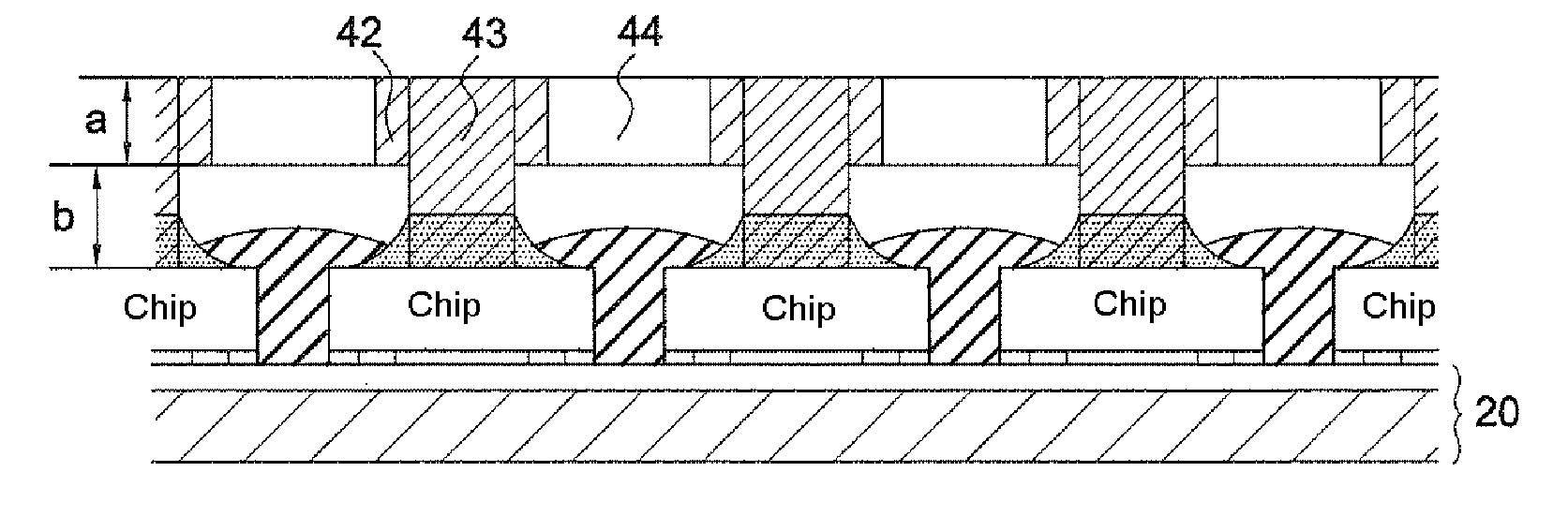
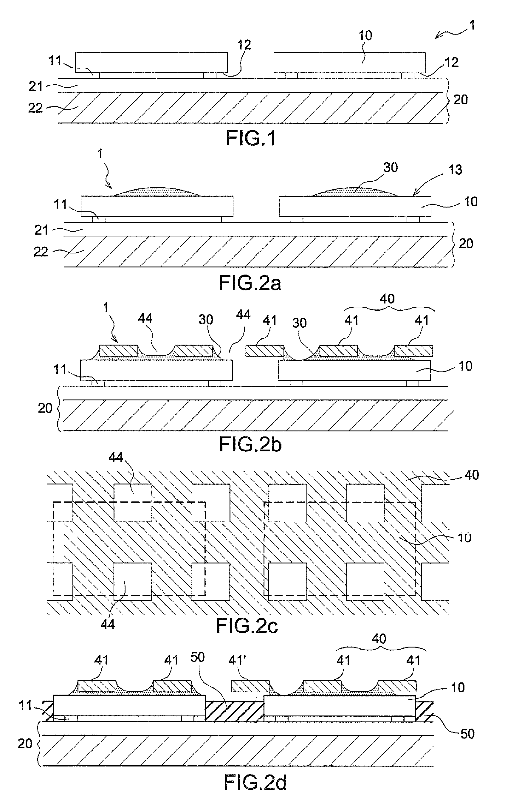
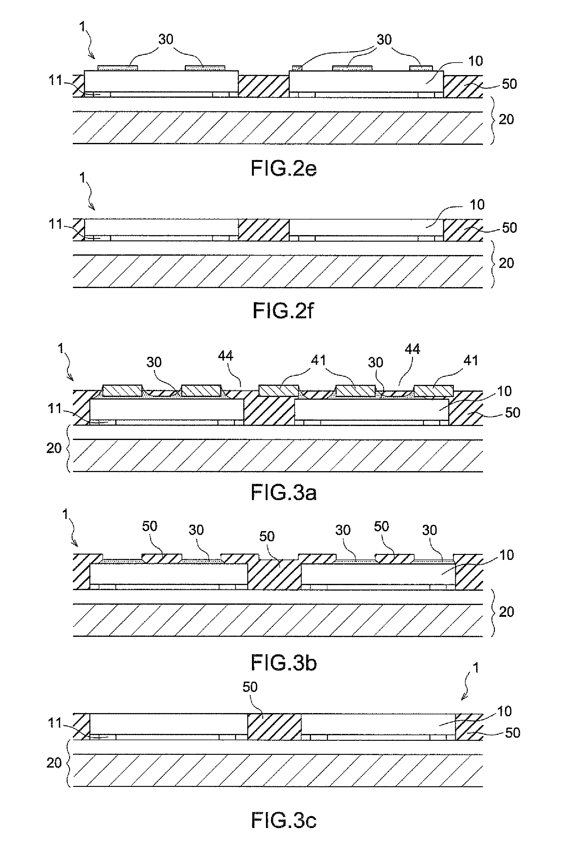
[0041]The process according to the invention is based on the use of a support wafer. Unlike the lattice of the prior art, the support wafer is bonded to the chips on the back side or, according to a variant, on the front side.

[0042]The support wafer may be made of copper or aluminum, these materials having an expansion coefficient of between 15 and 25 ppm / ° C.

[0043]Preferably, the material of the support wafer has an expansion coefficient close to that of the chips (in fact that of the main material of the chips) so as to expand approximately in the same way while the resin is curing, thus maintaining the positions prior to curing. Silicon, which is typically the material of the chips, has an expansion coefficient of about 3 to 4 ppm / ° C. A support wafer made of a material having an expansion coefficient of less than 10 ppm / ° C., such as ferro-nickel, would be preferably suitable. A support wafer made of silicon may also be envisaged.

[0044]The generally metallic support wafer may be...


PUM


Abstract

A process for fabricating a reconstituted wafer that includes chips having connection pads on a front side of the chip, this process including positioning of the chips on an adhesive support, front side down on the support; deposition of a resin on the support in order to encapsulate the chips; and curing of the resin. Before deposition of the resin, the process includes bonding, onto the chips, a support wafer for positioning the chips, this support wafer having parts placed on one side of the chips.

Description

CROSS-REFERENCE TO RELATED APPLICATIONS[0001]This application is a National Stage of International patent application PCT / EP2010 / 052964, filed on Mar. 9, 2010, which claims priority to foreign French patent application No. FR 09 01095, filed on Mar. 10, 2009, the disclosures of each of which are incorporated by reference in their entireties.FIELD OF THE INVENTION[0002]The field of the invention is that of the fabrication of reconstituted wafers comprising chips encapsulated in a resin, these chips generally having been tested beforehand.BACKGROUND OF THE INVENTION[0003]The solution most commonly employed for producing a reconstituted wafer consists in removing various types of chips or dies that are generally selected after having been tested and usually designated as “known good dies”. The term “chip” denotes an active electronic component, such as a bare chip, or a passive component or an MEMS (MicroElectroMechanical System). As shown in FIG. 1, these chips 10, which have connecti...

Claims


Application Information

Patent Timeline
IPC IPC(8): H01L21/00
CPCH01L21/561H01L21/6836H01L23/4334H01L24/96H01L25/0657H01L25/105H01L25/50H01L24/24H01L24/97H01L21/568H01L2224/24998H01L2221/68327H01L2225/06527H01L2225/06551H01L2225/06589H01L2924/01013H01L2924/01029H01L2924/01047H01L2924/01057H01L2924/01058H01L2924/01061H01L2924/01079H01L2924/09701H01L2924/01005H01L2924/01006H01L2924/01019H01L2924/01033H01L2924/01074H01L2924/01075H01L2225/1023H01L2225/1064H01L2225/1094H01L2224/24137H01L2224/32245H01L2224/73217H01L2224/92144H01L2224/97H01L2924/18162H01L2924/1461H01L2224/83H01L2224/82H01L2924/00H01L2924/181H01L21/56H01L21/563
Inventor VAL, CHRISTIAN
Owner 3D PLUS
Why Eureka
Try Eureka