Transistor device with reduced gate resistance

a transistor and gate resistance technology, applied in the field of semiconductor devices, to achieve the effect of reducing the gate resistan

Inactive Publication Date: 2013-10-15
INT BUSINESS MASCH CORP
View PDF20 Cites 29 Cited by
  • Summary
  • Abstract
  • Description
  • Claims
  • Application Information

AI Technical Summary

Problems solved by technology

The mushroom-like gate structure attempts to reduce gate resistance by adding material to the gate electrode, but may in some instances contribute to capacitance parasitics with surrounding metal structures.

Method used


Image

  • Transistor device with reduced gate resistance
  • Transistor device with reduced gate resistance
  • Transistor device with reduced gate resistance

Examples


Embodiment Construction

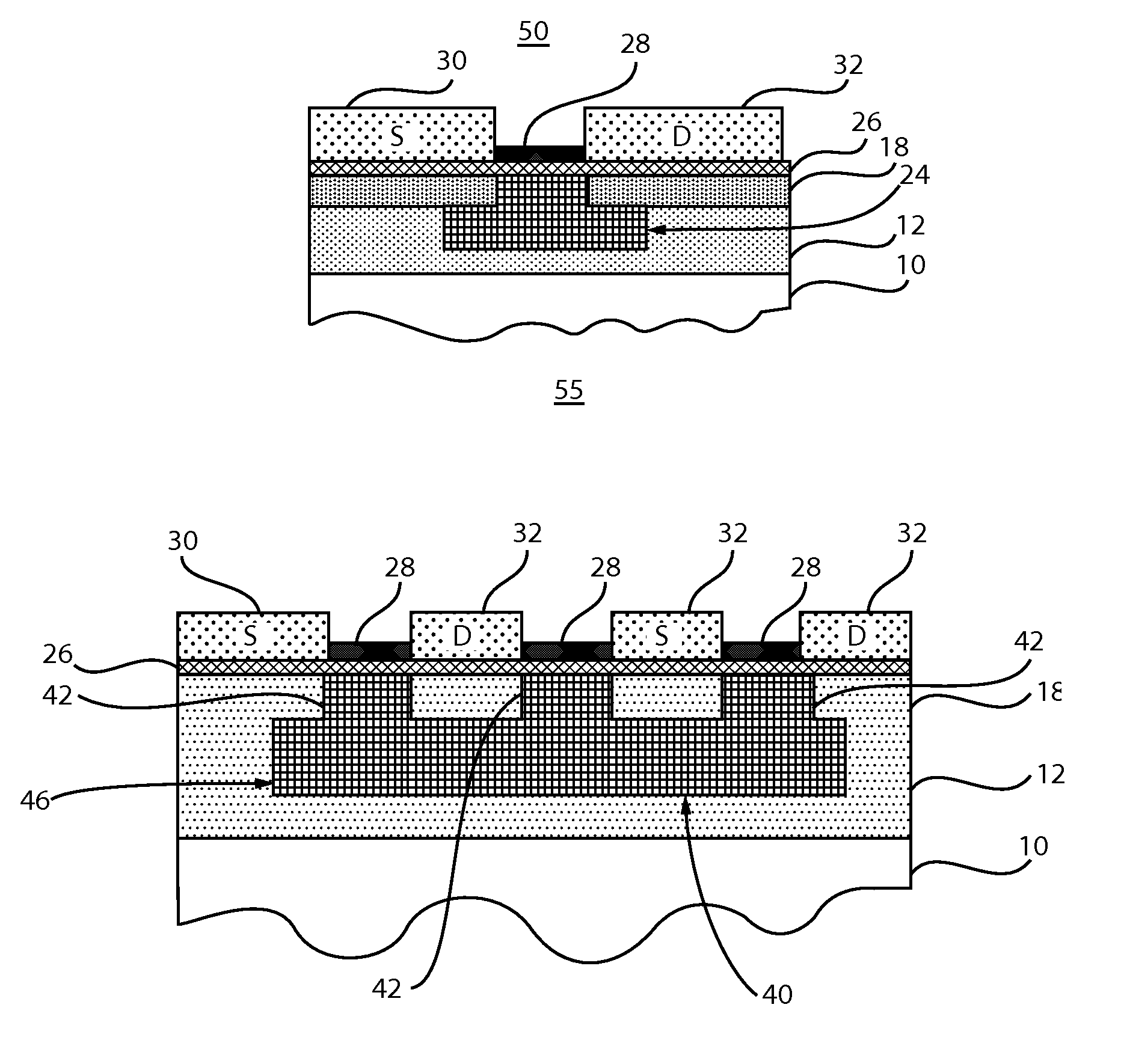
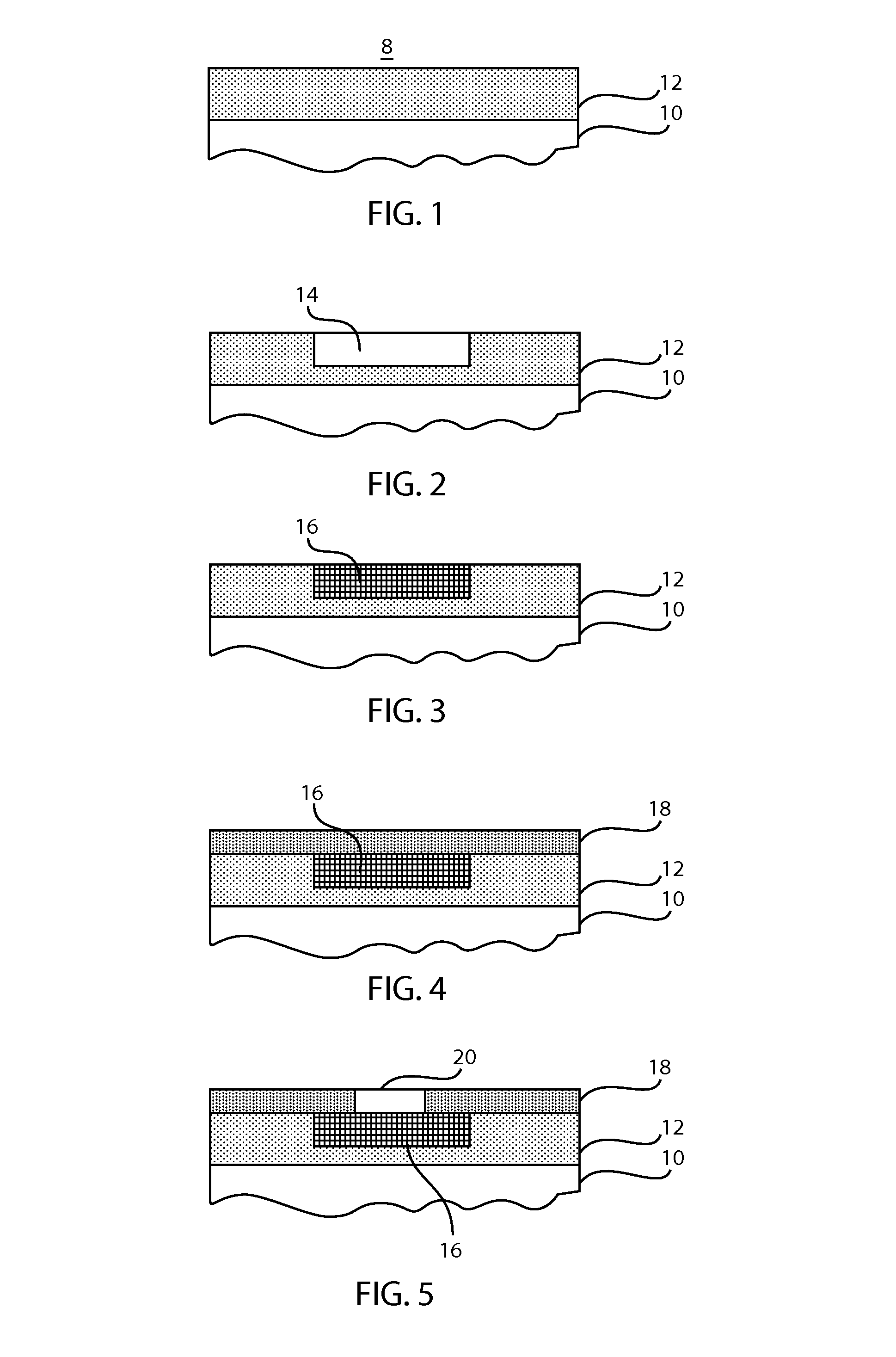
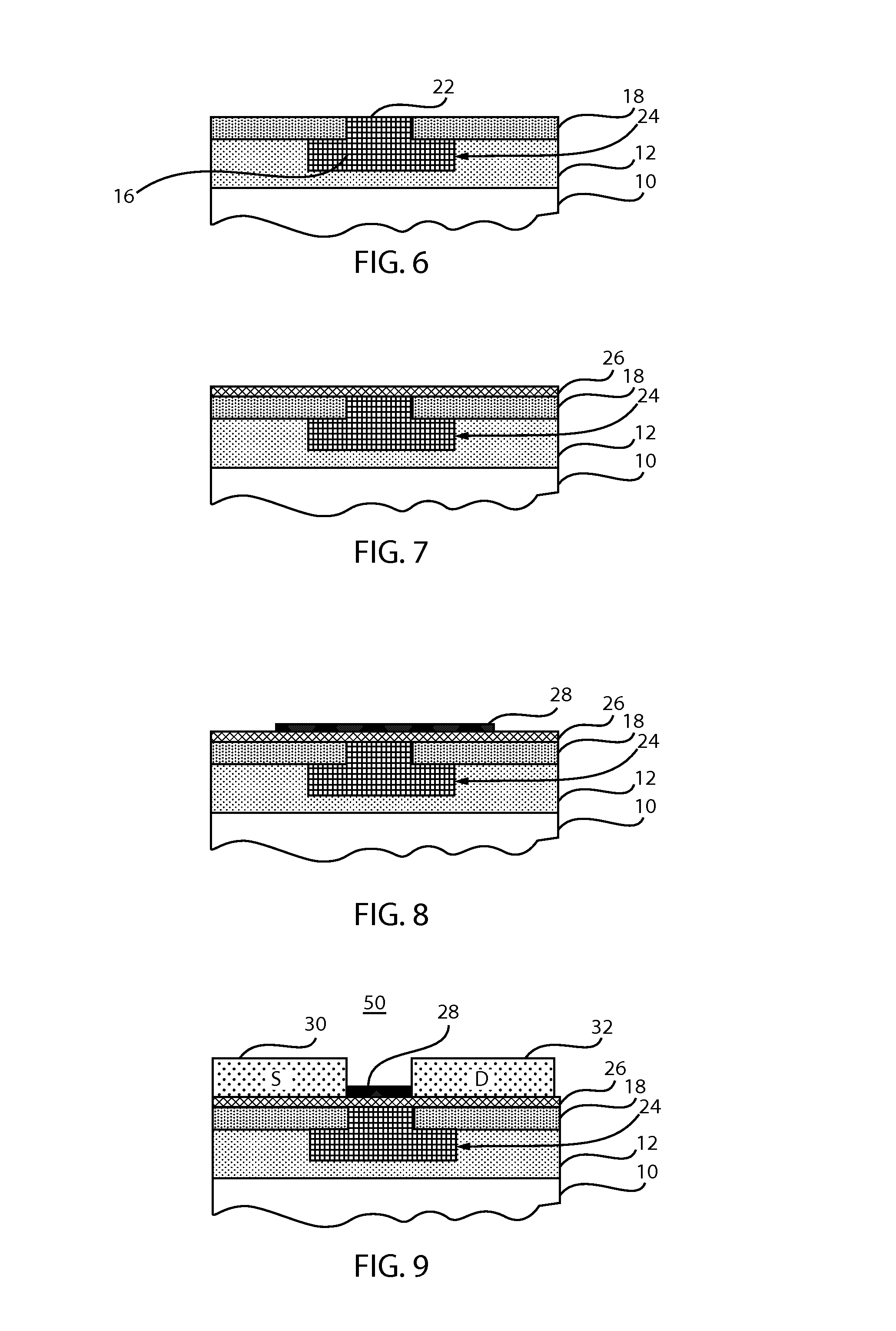
[0022]In accordance with the present principles, gate structures, devices and methods for fabrication are provided having reduced gate resistance without additional capacitive parasitics. Particularly useful embodiments include an embedded gate structure. The embedded gate structure includes a structure where a conductive channel layer is formed over the gate structure. The channel layers include graphene, carbon nanotubes, or any kind of semiconducting material, preferably a material that is transferable. In one embodiment, the gate structures are formed, followed by the conductive / semi-conductive channel layer, and then source and drain regions are formed on the channel layer. The gate structure includes additional material and may take the form of an inverted “T” shape, although other shapes like an “L” shape, etc. may be employed.

[0023]In one embodiment, the conductive channel layer includes an electrically conductive carbon material (which may be transferable over the gate stru...


PUM


Abstract

A device with reduced gate resistance includes a gate structure having a first conductive portion and a second conductive portion formed in electrical contact with the first conductive portion and extending laterally beyond the first conductive portion. The gate structure is embedded in a dielectric material and has a gate dielectric on the first conductive portion. A channel layer is provided over the first conductive portion. Source and drain electrodes are formed on opposite end portions of a channel region of the channel layer. Methods for forming a device with reduced gate resistance are also provided.

Description

BACKGROUND[0001]1. Technical Field[0002]The present invention relates to semiconductor devices, and more particularly to devices with a gate structure with reduced gate resistance and methods for fabricating the same.[0003]2. Description of the Related Art[0004]Conventional top-gated field effect transistors (FET) include a number of associated parasitics. With continuous gate-length scaling associated with denser device layouts, FET gate resistance increases. As a result, maximum oscillating frequency (fMAX) performance of complementary metal oxide semiconductor (CMOS) FETs has improved little beyond the 45 nm node. With conventional CMOS fabrication techniques, gate resistance can only be reduced by using multiple fingers, decreasing device width or employing a double-contacted gate structure. In such devices, additional metal layers (with lower resistance than poly-silicon) can make contact with a gate node only outside of the device area to reduce parasitic capacitances to make ...

Claims


Application Information

Patent Timeline
Patent Type & Authority Patents(United States)
IPC IPC(8): H01L21/00H01L21/44H01L21/336H01L21/84H01L29/786
CPCH01L29/42384H01L29/66742H01L29/78603H01L29/78636H01L29/78684H01L29/7781
Inventor HAN, SHU-JENVALDES GARCIA, ALBERTO
Owner INT BUSINESS MASCH CORP
Why Eureka
Try Eureka