Semiconductor device and production method thereof

a technology of semiconductor and production method, which is applied in the direction of semiconductor/solid-state device manufacturing, transistors, electrical equipment, etc., can solve the problems of inability to reduce the area occupied by the circuit, difficulty in controlling the leak current, and inability to flow current, etc., to achieve low and stable contact resistance

Active Publication Date: 2013-10-22
UNISANTIS ELECTRONICS SINGAPORE PTE LTD
View PDF24 Cites 8 Cited by
  • Summary
  • Abstract
  • Description
  • Claims
  • Application Information

AI Technical Summary

Benefits of technology

[0007]The purpose of the present application is to provide a structure of a contact layer preventing short circuits between the contact layer on a columnar semiconductor layer and the gate electrode formed around the columnar semiconductor layer and obtaining low and stable contact resistance, and a production method thereof.
[0088]According to the present invention, it is possible in a vertical transistor to prevent short circuits between a contact layer on a columnar semiconductor layer and a gate electrode formed around the columnar semiconductor layer. Furthermore, according to the present invention, it is possible to obtain low and stable contact resistance.

Problems solved by technology

As MOS transistors become smaller, problems occur such as difficulty in controlling the leak current and difficulty in reducing the area occupied by the circuits while assuring a necessary current quantity.
However, because it is difficult to apply a voltage on the source and drain in accordance with the desired current when the source and drain have high resistance, the desired current cannot flow.
In this case, if over-etching occurs during forming contact holes by etching in the step of forming a contact layer on the columnar semiconductor layer, short circuits between the contact layer on the columnar semiconductor layer and the gate electrode formed around the columnar semiconductor layer may easily occur.

Method used


Image

  • Semiconductor device and production method thereof
  • Semiconductor device and production method thereof
  • Semiconductor device and production method thereof

Examples


Embodiment Construction

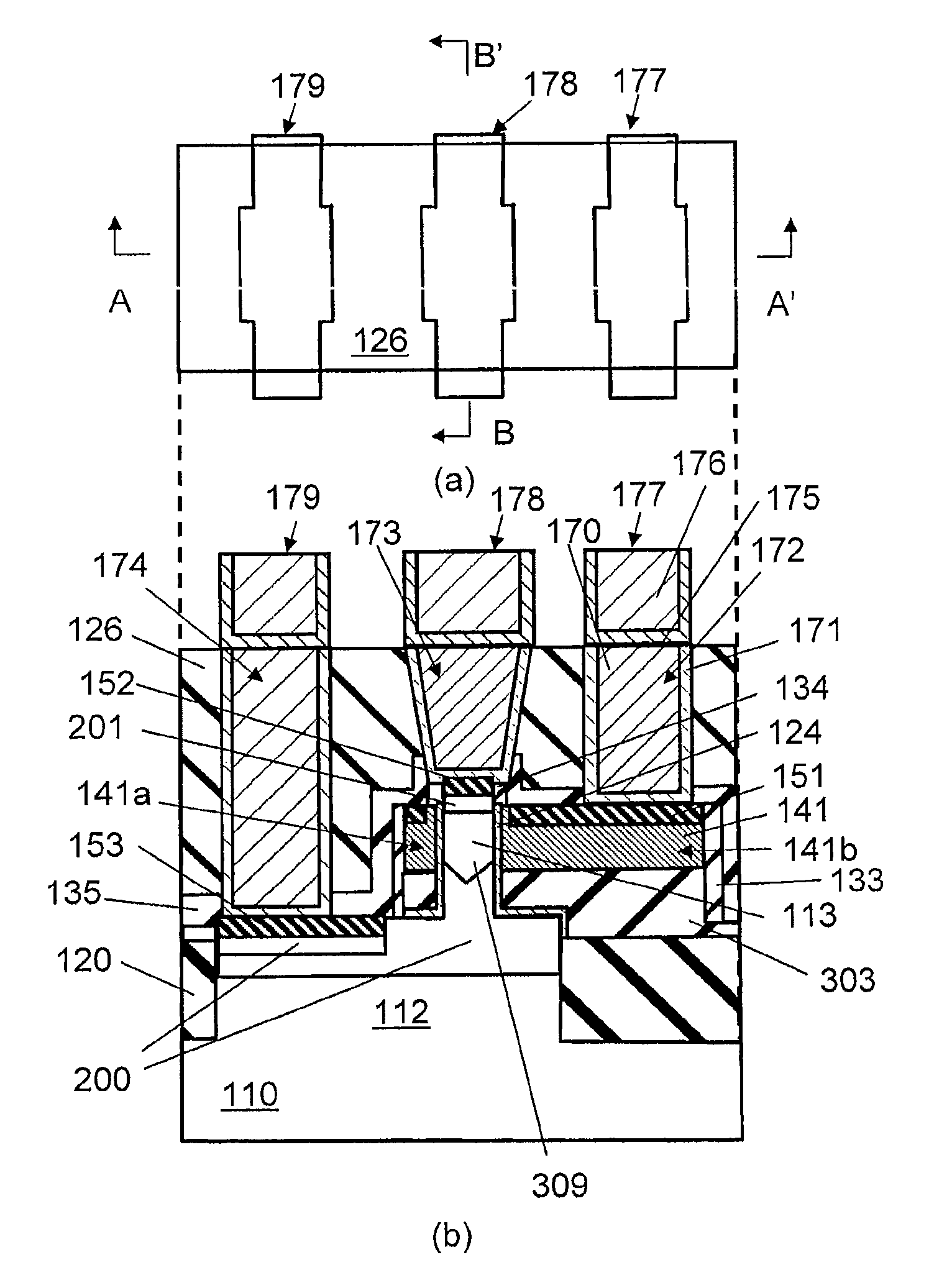
[0144]FIG. 43 is a drawing showing an NMOS SGT of a semiconductor device according to a first embodiment of, with part (a) showing a planar view and part (b) showing a cross-sectional view along the cut line A-A′ in part (a). FIG. 44 is a cross-sectional view along the cut line B-B′ in the planar view (a). An NMOS SGT of a semiconductor device according to the first embodiment is described hereafter with reference to FIGS. 43 and 44.

[0145]A planar silicon layer 112 that is the planar semiconductor layer is formed on a silicon substrate 110 that is the substrate. A columnar silicon layer 113 that is the columnar semiconductor layer is formed on the planar silicon layer 112. A source diffusion layer 200 is formed in the lower part of the columnar silicon layer 113 and in the planar silicon layer 112. A drain diffusion layer 201 is formed in the upper part of the columnar silicon layer 113. A body 309 is formed between the source diffusion layer 200 and the drain diffusion layer 201. A...


PUM


Abstract

A method for producing a semiconductor device includes preparing a structure having a substrate, a planar semiconductor layer and a columnar semiconductor layer, forming a second drain / source region in the upper part of the columnar semiconductor layer, forming a contact stopper film and a contact interlayer film, and forming a contact layer on the second drain / source region. The step for forming the contact layer includes forming a pattern and etching the contact interlayer film to the contact stopper film using the pattern to form a contact hole for the contact layer and removing the contact stopper film remaining at the bottom of the contact hole by etching. The projection of the bottom surface of the contact hole onto the substrate is within the circumference of the projected profile of the contact stopper film formed on the top and side surface of the columnar semiconductor layer onto the substrate.

Description

CROSS-REFERENCE TO RELATED APPLICATION[0001]This application is a divisional patent application of U.S. Ser. No. 12 / 858,840, filed Aug. 18, 2010, which claims the benefit of Japanese Patent Application No. 2009-189262 filed on Aug. 18, 2009 and U.S. Provisional Application No. 61 / 274,733 filed on Aug. 19, 2009, and the entire disclosure of each is incorporated by reference herein.[0002]This application relates generally to a semiconductor device and production method thereof.BACKGROUND OF THE INVENTION[0003]Semiconductor integrated circuits, particularly integrated circuits using MOS transistors, have increasingly been highly integrated. MOS transistors in integrated circuits have been downsized to nano sizes as the integration level is increased. As MOS transistors become smaller, problems occur such as difficulty in controlling the leak current and difficulty in reducing the area occupied by the circuits while assuring a necessary current quantity. In order to resolve these proble...

Claims


Application Information

Patent Timeline
Patent Type & Authority Patents(United States)
IPC IPC(8): H01L21/336
CPCH01L21/76804H01L21/76816H01L29/41741H01L29/42356H01L29/66666H01L29/7827H01L21/768H01L21/823487H01L27/088H01L29/045H01L29/0696H01L29/42368H01L29/4238H01L29/66348H01L29/7397H01L29/7813H01L29/7815
Inventor MASUOKA, FUJIOARAI, SHINTARONAKAMURA, HIROKIKUDO, TOMOHIKOMURTHY, R. RAMANASHEN, NANSHENGBUDDHARAJU, KAVITHA DEVISINGH, NAVAB
Owner UNISANTIS ELECTRONICS SINGAPORE PTE LTD
Why Eureka
Try Eureka