Printed wiring board assembly and related methods

a printed wiring board and assembly technology, applied in the field of circuit boards, can solve the problems of increasing the size of assembled circuit boards, interconnecting circuit boards, installation drawbacks, etc., and achieve the effect of cost-effective and efficient manufacturing

Active Publication Date: 2013-11-05
HARRIS CORP
View PDF20 Cites 7 Cited by
  • Summary
  • Abstract
  • Description
  • Claims
  • Application Information

AI Technical Summary

Benefits of technology

[0007]In view of the foregoing background, it is therefore an object of the present invention to provide a method for making a printed wiring board (PWB) assembly that is cost effective and efficiently manufactured.
[0008]This and other objects, features, and advantages in accordance with the present invention are provided by a method that may include forming a first PWB having a plurality of first electrically conductive pads, forming a second PWB including a plurality of electrically conductive traces having exposed ends on an edge surface of the second PWB, and covering the edge surface of the second PWB with an electrically conductive layer. The method may also include selectively removing portions of the electrically conductive layer to define a plurality of second electrically conductive pads electrically connected to corresponding ones of the exposed ends of the electrically conductive traces, and assembling the first and second PWBs together so that the first and second electrically conductive pads are electrically coupled together to define the PWB assembly. Advantageously, the PWB assembly may use less packaging and may be more efficiently manufactured.

Problems solved by technology

The use of the interconnector component may increase the size of the assembled circuit boards.
This may pose installation drawbacks in applications where space may be limited.
One approach to the above drawback is to interconnect circuit boards without using a separate interconnector component.
One drawback of the Hash et al. method is the expense per unit for manufacturing may be high.
Moreover, the vias for each of the layers need to be accurately aligned, adding a possible drawback to robust fabrication.

Method used


Image

  • Printed wiring board assembly and related methods
  • Printed wiring board assembly and related methods
  • Printed wiring board assembly and related methods

Examples


Embodiment Construction

[0019]The present invention will now be described more fully hereinafter with reference to the accompanying drawings, in which preferred embodiments of the invention are shown. This invention may, however, be embodied in many different forms and should not be construed as limited to the embodiments set forth herein. Rather, these embodiments are provided so that this disclosure will be thorough and complete, and will fully convey the scope of the invention to those skilled in the art. Like numbers refer to like elements throughout, and multiple prime notation is used to indicate similar elements in alternative embodiments.

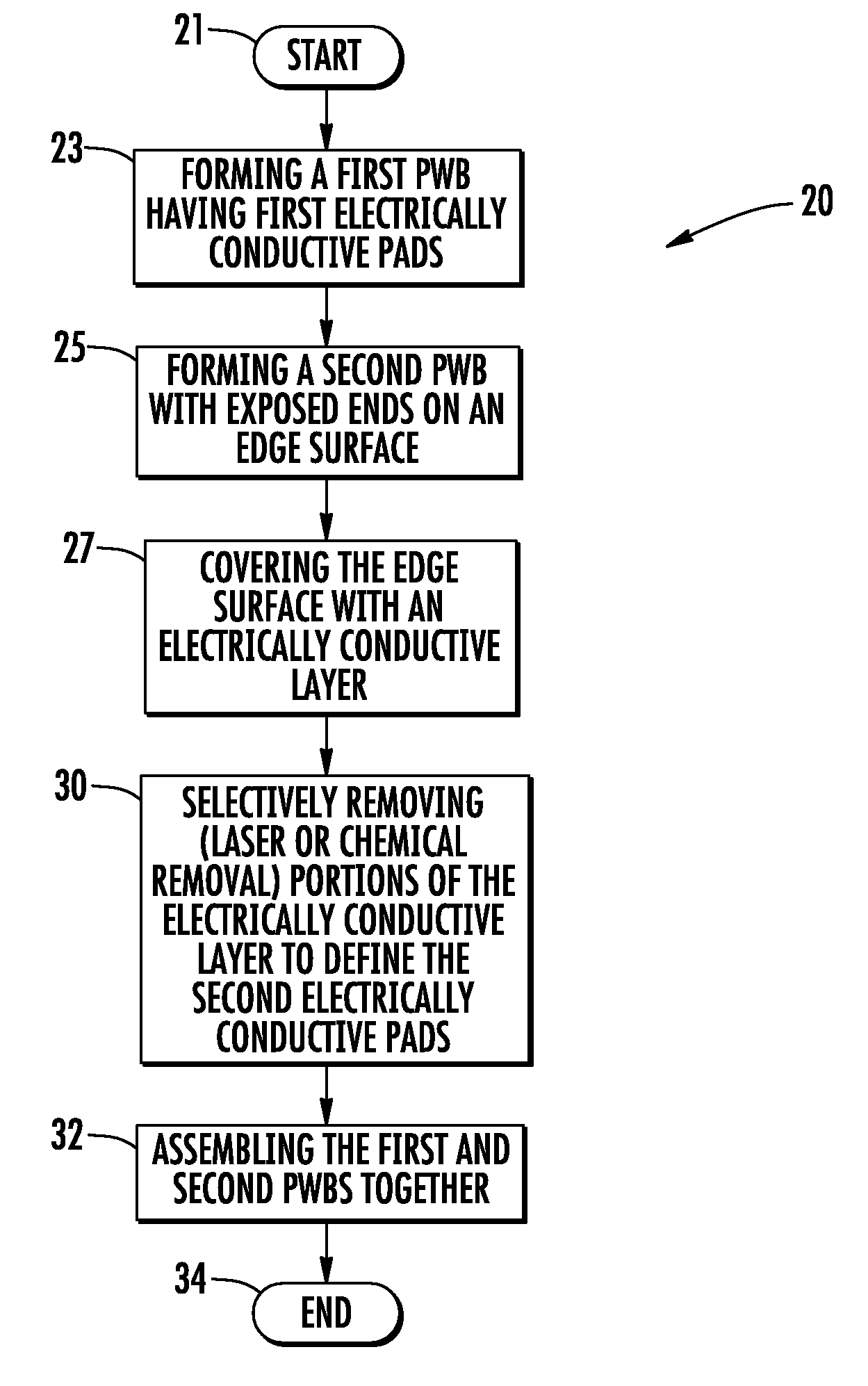
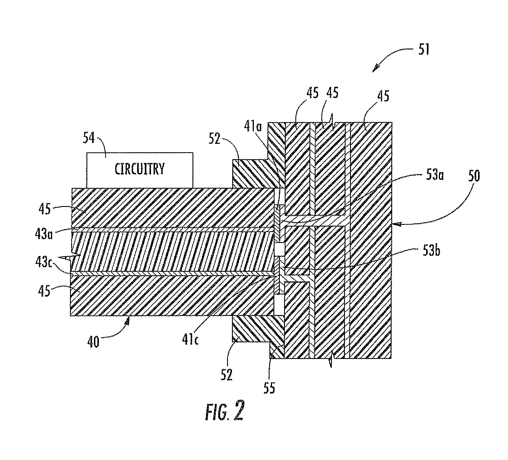
[0020]Referring initially to FIGS. 1-3, a flowchart 20 illustrates a method for making a printed wiring board (PWB) assembly 51 that begins at Block 21. The method illustratively includes at Block 23 forming a first PWB 50 having a plurality of first electrically conductive pads 53a-53d. The first electrically conductive pads 53a-53d (only two of which are visible ...


PUM

PropertyMeasurementUnit
electrically conductiveaaaaaaaaaa
widthaaaaaaaaaa
planar shapeaaaaaaaaaa

Abstract

A method is for making a printed wiring board (PWB) assembly. The method may include forming a first PWB having a plurality of first electrically conductive pads, forming a second PWB including a plurality of electrically conductive traces having exposed ends on an edge surface of the second PWB, and covering the edge surface of the second PWB with an electrically conductive layer. The method may also include selectively removing portions of the electrically conductive layer to define a plurality of second electrically conductive pads electrically connected to corresponding ones of the exposed ends of the electrically conductive traces, and assembling the first and second PWBs together so that the first and second electrically conductive pads are electrically coupled together to define the PWB assembly.

Description

FIELD OF THE INVENTION[0001]The present invention relates to the field of circuit boards, and, more particularly, to assembled printed wiring boards and related methods.BACKGROUND OF THE INVENTION[0002]An electronic device may include one or more circuit boards. A typical circuit board is a planar board that mechanically supports electronic components. The electronic components may comprise, for example, resistors, capacitors, switches, batteries, and other more complex integrated circuit components, i.e. microprocessors. The circuit board typically comprises a dielectric material, for example, a plastic material.[0003]A simple circuit board may include conductive traces on its surface for connecting the electronic components to each other. As electronic circuitry has become more complex, multi-layer circuit boards with at least two electrically conductive trace layers sandwiched between dielectric layers have been developed. Typically, the different conductive trace layers of a mul...

Claims


Application Information

Patent Timeline
Patent Type & Authority Patents(United States)
IPC IPC(8): H05K3/30
CPCH05K3/366H05K3/403H05K1/144H05K1/111H05K1/117H05K1/0219H05K1/142H05K3/301H05K2201/0919H05K2201/10446H05K2201/09809H05K2201/09145H05K2201/09481Y10T29/4913Y10T29/49126Y10T29/49155Y10T29/49133
Inventor PEDERSEN, ANDERS P.ROBISON, DANIEL A.MAST, ALAN W.
Owner HARRIS CORP
Why Eureka
Try Eureka