MEMS fabrication process base on SU-8 masking layers

a technology of micro-electromechanical systems and masking layers, applied in the direction of microlithography exposure apparatus, photomechanical treatment, instruments, etc., can solve the problems of wasting time and money, affecting the quality of the mask, and requiring approximately 1 week to write, fabricate, and ship new negative tone masks with 2 m minimum features, etc., to achieve the effect of saving both money and tim

Inactive Publication Date: 2013-11-05
UNITED STATES OF AMERICA
View PDF0 Cites 8 Cited by
  • Summary
  • Abstract
  • Description
  • Claims
  • Application Information

AI Technical Summary

Benefits of technology

[0006]A novel processing technique has been developed that uses a combination of negative and positive photoresists for use with positive photomasks, resulting in masking layers suitable for bulk micromachining in the fabrication of microelectromechanical systems (MEMS). This technique allows for the use of positive photomasks with negative resists, which opens the door to the ability to create com...

Problems solved by technology

Often times, however, in university-based, sponsor-funded research, funding is simply not available to purchase new masks while device fabrication is on-going.
For example, a new negative tone mask with 2 μm minimum...

Method used


Image

  • MEMS fabrication process base on SU-8 masking layers
  • MEMS fabrication process base on SU-8 masking layers
  • MEMS fabrication process base on SU-8 masking layers

Examples


Embodiment Construction

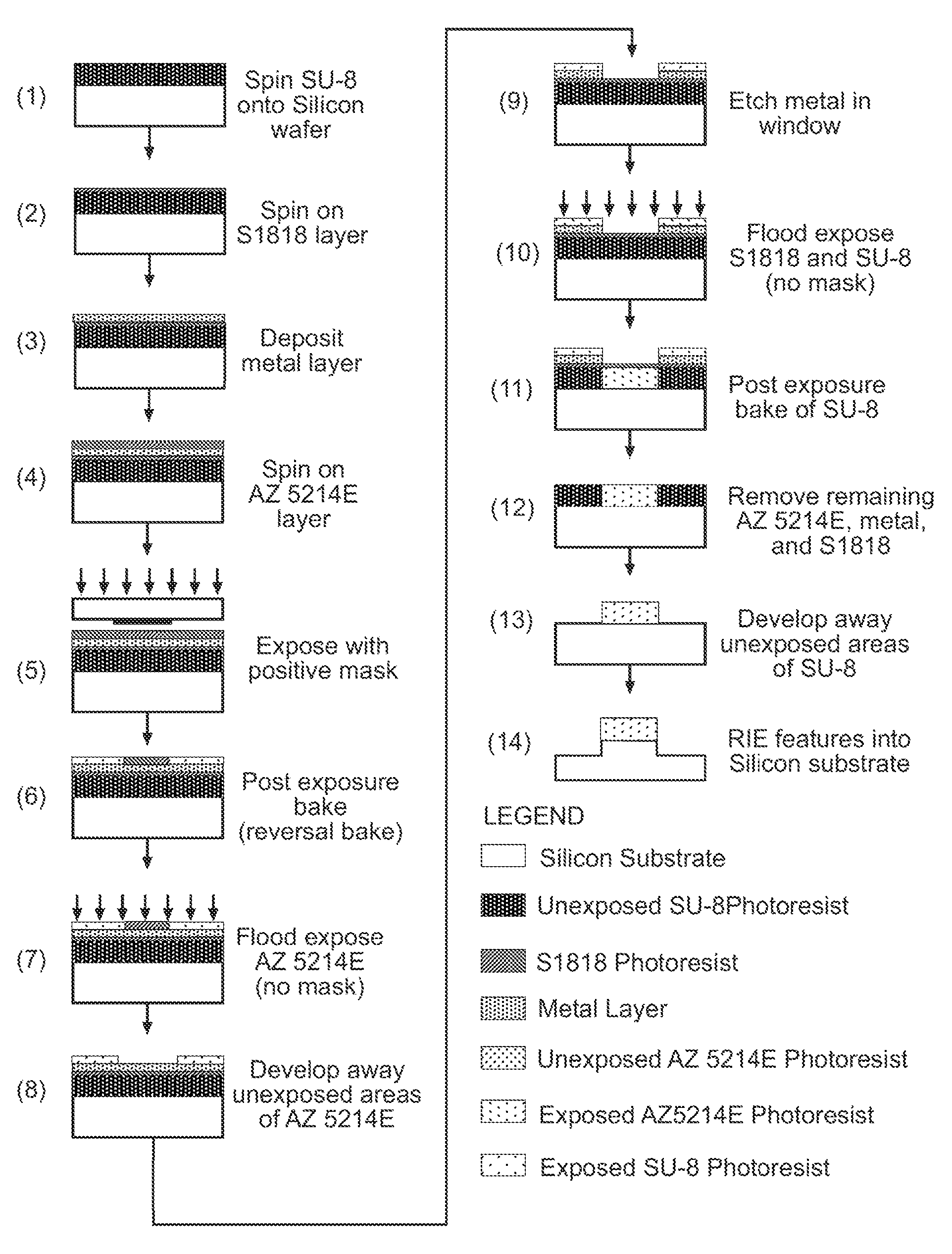
[0025]This processing technique has been detailed in: (1) Scott A. Ostrow II, Jack P. Lombardi III and Ronald A. Coutu, Jr., “Using positive photomasks to pattern SU-8 masking layers for fabricating inverse MEMS structures”, Proc. SPIE 7972, 79722J (2011); doi:10.1117 / 12.881653; and, (2) Scott A. Ostrow and Jr. Ronald A. Coutu, “Novel microelectromechanical systems image reversal fabrication process based on robust SU-8 masking layers”, J. Micro / Nanolith. MEMS MOEMS 10, 033016 (Sep. 2, 2011); doi:10.1117 / 1.3625633, both of which are incorrorated herein by reference.

[0026]The process starts with the coating of a clean silicon wafer with SU-8 at the standard spin speeds. A 5-μm thick SU-8 layer was utilized in the development of this novel process. This is followed by a ramped softbake, with a bake at 65° C. for 3 min. followed by a bake at 110° C. for 10 min. This is a longer bake time and higher bake temperature than typically prescribed, but it is critical to ensure the integrity o...


PUM


Abstract

A novel fabrication process uses a combination of negative and positive photoresists with positive tone photomasks, resulting in masking layers suitable for bulk micromachining high-aspect ratio microelectromechanical systems (MEMS) devices. This technique allows the use of positive photomasks with negative resists, opening the door to an ability to create complementary mechanical structures without the fabrication delays and costs associated with having to obtain a negative photomask. In addition, whereas an SU-8 mask would normally be left in place after processing, a technique utilizing a positive photoresist as a release layer has been developed so that the SU-8 masking material can be removed post-etching.

Description

RIGHTS OF THE GOVERNMENT[0001]The invention described herein may be manufactured and used by or for the Government of the United States for all governmental purposes without the payment of any royalty.BACKGROUND OF THE INVENTION[0002]The invention relates to microelectromechanical systems and microfabrication.[0003]Photolithography is an iterative process used to transfer patterns from a photomask design onto a photosensitive material or photoresist. Once transferred into the photoresist, the pattern is then developed and “windows” to the underlying material are opened up. The underlying materials are then etched away, leaving behind a permanent pattern in the lower material, or materials are deposited into the windows. When fabricating surface micromachined microelectromechanical systems (MEMS) devices, thin film depositions are interlaced with photolithography, etching, and lift-off processing steps. Typically, positive photomasks and photoresists are used in MEMS fabrication to e...

Claims


Application Information

Patent Timeline
IPC IPC(8): G03F7/20
CPCG03F7/038G03F7/2022G03F7/2016G03F7/095
Inventor OSTROW, II, SCOTT ACOUTU, JR., RONALD A
Owner UNITED STATES OF AMERICA
Why Eureka
Try Eureka