Optical semiconductor lighting apparatus

a technology of optical semiconductors and lighting equipment, which is applied in the direction of lighting and heating equipment, semiconductor devices for light sources, and support devices for lighting, etc., can solve the problems of increasing increasing the manufacturing cost and the amount of raw materials used, and inevitably generating heat from optical semiconductors. to achieve the effect of reducing the total weight of the produ

Inactive Publication Date: 2013-11-19
POSCO LED
View PDF20 Cites 14 Cited by
  • Summary
  • Abstract
  • Description
  • Claims
  • Application Information

AI Technical Summary

Benefits of technology

[0015]An aspect of the present invention is directed to provide an optical semiconductor lighting apparatus that can reduce a total weight of a product.
[0016]Another aspect of the present invention is directed to provide an optical semiconductor lighting apparatus that can further improve the heat dissipation efficiency by inducing natural convection.
[0017]Another aspect of the present invention is directed to provide an optical semiconductor lighting apparatus that is simple in the product assembly and installation and is easy in maintenance.
[0018]Another aspect of the present invention is directed to provide an optical semiconductor lighting apparatus that can provide products with high reliability by increasing the arrangement efficiency of semiconductor optical devices per unit area.

Problems solved by technology

Typically, in the lighting apparatuses using such optical semiconductors, heat is inevitably generated from the optical semiconductors.
However, the heat sinks manufactured in such a manner increase the total weight of the product and increase the manufacturing costs and the amount of raw materials used.
In particular, in the case of the conventional heat sinks manufactured by die casting, heat sink fins cannot be formed to have a thickness below a predetermined reference value due to characteristics of the manufacturing method thereof.
However, due to the structural limitation that the heat sink should be arranged in a line contact manner, heat generated from optical semiconductors may not be effectively transferred and discharged to the outside.

Method used


Image

  • Optical semiconductor lighting apparatus
  • Optical semiconductor lighting apparatus
  • Optical semiconductor lighting apparatus

Examples


Embodiment Construction

[0053]Exemplary embodiments of the present invention will be described below in detail with reference to the accompanying drawings.

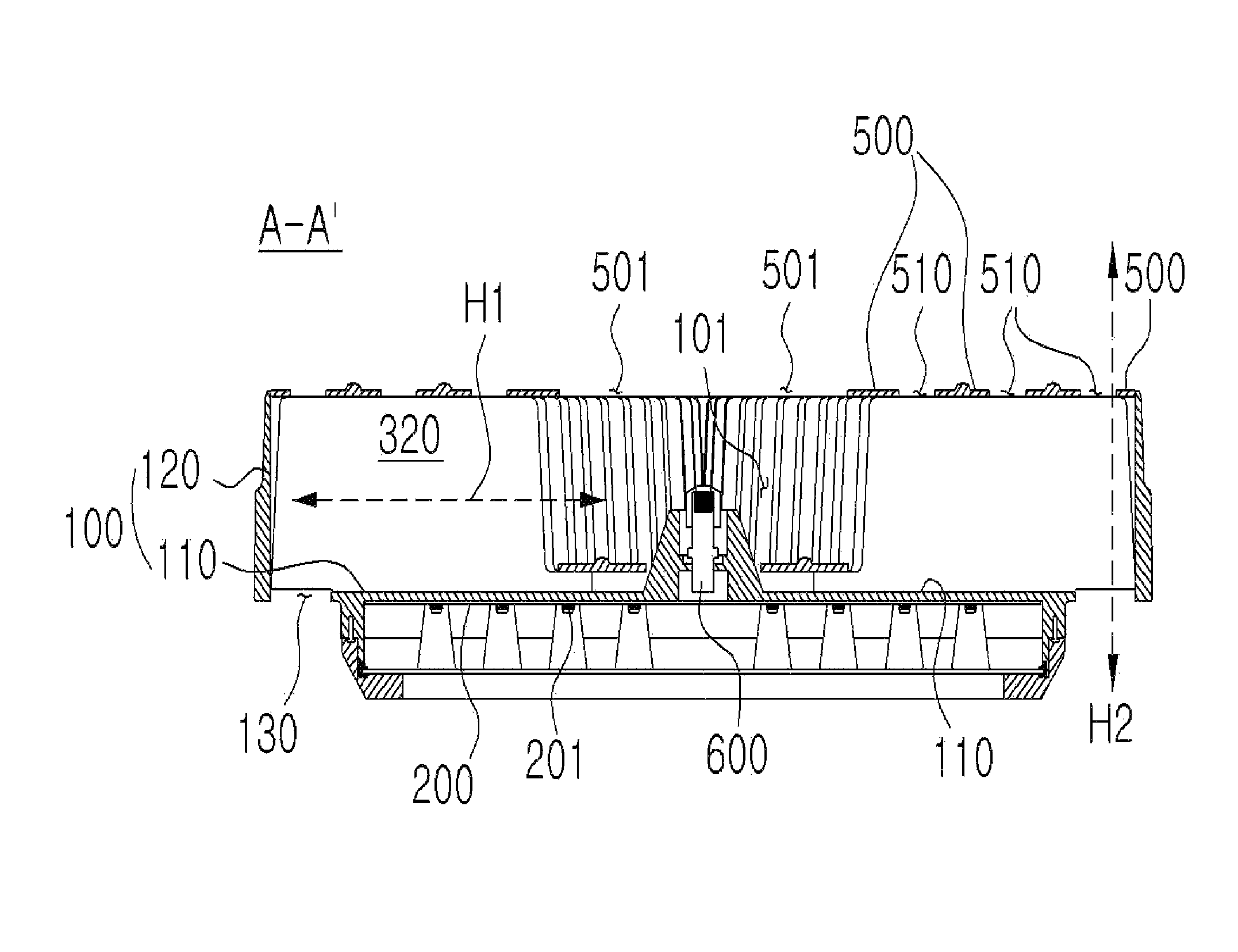
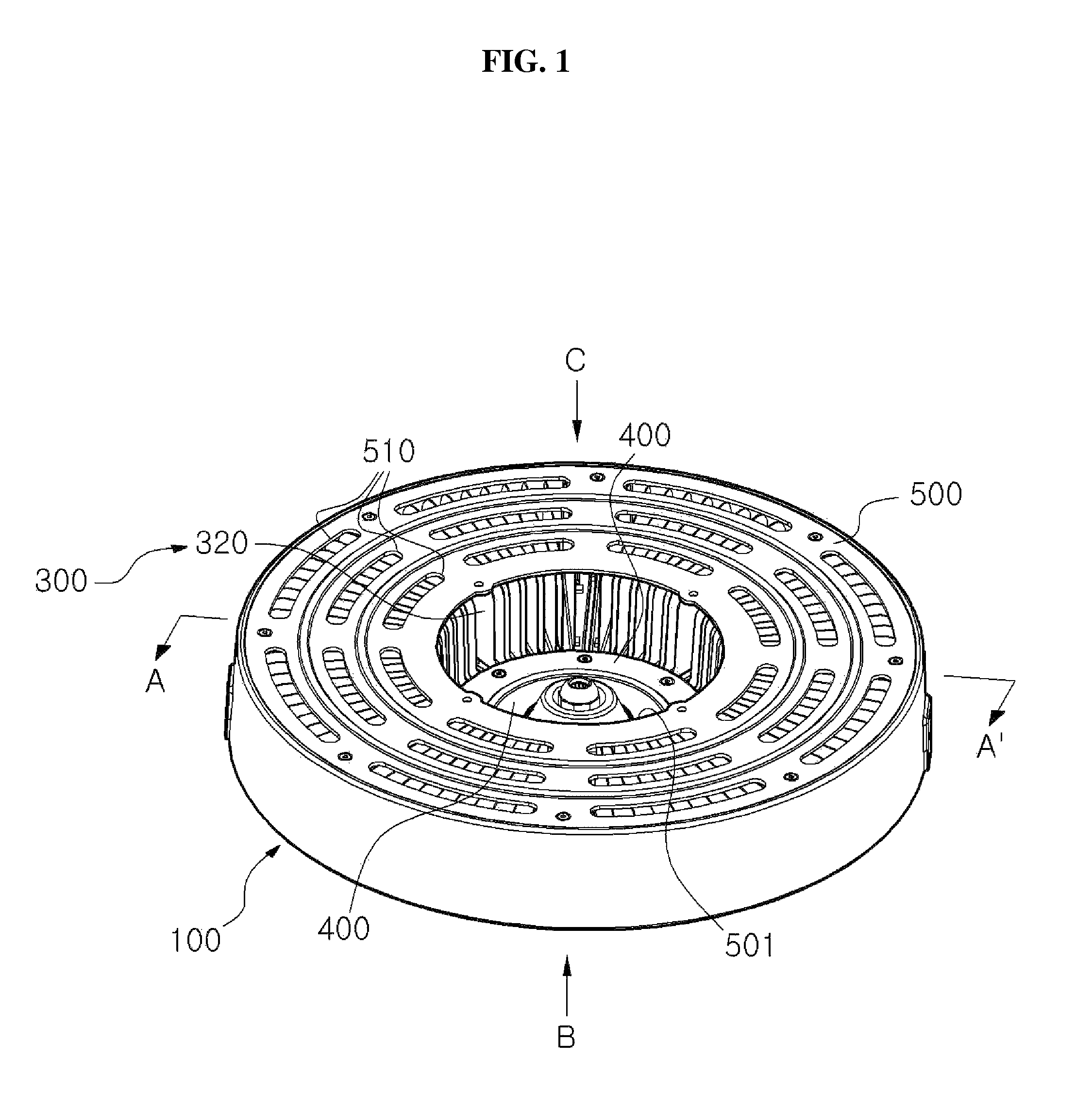
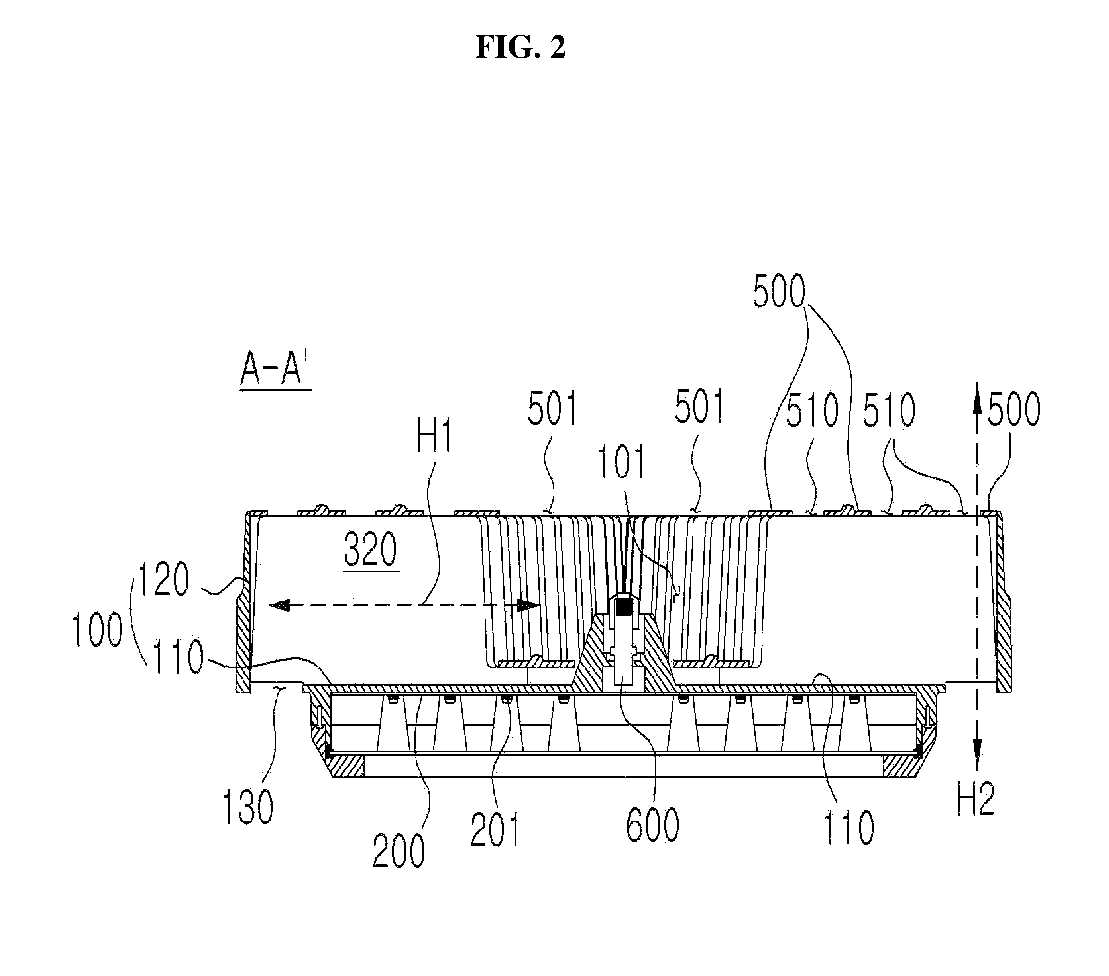
[0054]FIG. 1 is a perspective view illustrating an overall configuration of an optical semiconductor lighting apparatus according to an embodiment of the present invention. FIG. 2 is a cross-sectional view taken along line A-A′ of FIG. 1. FIG. 3 is a partial conceptual diagram viewed from a viewpoint B of FIG. 1. FIG. 4 is a partial conceptual diagram viewed from a viewpoint C of FIG. 1. FIGS. 5 to 6 are diagrams illustrating an overall configuration of a unit heat sink element constituting a heat sink unit that is an essential part of an optical semiconductor lighting apparatus according to an embodiment of the present invention.

[0055]As illustrated, the optical semiconductor lighting apparatus according to the embodiment of the present invention is configured such that a heat sink unit 300 is mounted on a housing 100 where a light emitting module 200 i...


PUM


Abstract

A first heat sinking path formed in a forming direction of a heat sink unit disposed radially in a housing where a light emitting module is mounted. A second heat sinking path is formed along an edge of the light emitting module. By providing a light engine concept in which a light emitting module, an optical member, and a heat sink unit are included and a bottom surface is gradually widened from one side to the other side, an optical semiconductor lighting apparatus can reduce a total weight of a product, can further improve heat dissipation efficiency by inducing natural convection, is simple in the product assembly and installation, and is easy in maintenance, and can provide products with high reliability by increasing the arrangement efficiency of semiconductor optical devices per unit area.

Description

CROSS-REFERENCE(S) TO RELATED APPLICATION[0001]This application claims priority of Korean Patent Application No. 2012-0075103, filed on Jul. 10, 2012, and Korean Patent Application No. 2012-0076852, filed on Jul. 13, 2012, which are hereby incorporated by reference in their entirety.BACKGROUND OF THE INVENTION[0002]1. Field of the Invention[0003]The present invention relates to an optical semiconductor lighting apparatus.[0004]2. Description of the Related Art[0005]Compared with incandescent light and fluorescent light, optical semiconductors, such as LEDs or LDs, consume low power, have a long lifespan, and have high durability and high brightness. Due to these advantages, optical semiconductors have recently attracted much attention as one of components for lighting.[0006]Typically, in the lighting apparatuses using such optical semiconductors, heat is inevitably generated from the optical semiconductors. Therefore, it is necessary to install heat sinks at heat generation sites so...

Claims


Application Information

Patent Timeline
Patent Type & Authority Patents(United States)
IPC IPC(8): F21V29/00
CPCF21V29/22F21V29/004F21V29/83F21V29/507F21V29/70F21V29/773F21V15/011F21Y2101/02F21Y2105/001F21Y2105/10F21Y2115/10F21V17/005
Inventor KIM, DONG SOOKANG, SEOK JINKIM, KYOO SEOKJANG, YOON GILKIM, DONG HEEYOON, SEONG BOKKIM, JUNG HWA
Owner POSCO LED
Why Eureka
Try Eureka