Multiple wavelength LED array illuminator for fluorescence microscopy

a led array and fluorescence microscopy technology, which is applied in the direction of lighting and heating apparatuses, lighting support devices, instruments, etc., can solve the problems of high energy consumption, large unused light output from lamps, and difficult simultaneous achievement of all these criteria, and achieve large numerical apertures, large apertures and diameters, and high spatial uniformity.

Active Publication Date: 2013-12-03
DICON FIBEROPTICS
View PDF48 Cites 9 Cited by
  • Summary
  • Abstract
  • Description
  • Claims
  • Application Information

AI Technical Summary

Benefits of technology

[0008]One embodiment of the invention is directed to a multiple wavelength LED array illuminator for providing light along an optical axis, which comprises a substrate and at least one array of multiple LED chips without individual packaging supported by the substrate, wherein the LED chips emit light within different wavelength ranges and are distributed laterally with respect to the axis over an area, the LED chips having light emitting surfaces for emitting light in directions transverse to the area. The illuminator includes an optical element adjacent to the light emitting surfaces of the LED chips in the at least one array that collects and directs light emitted by the LED chips of the at least one array along the axis towards a target. Additional optical elements, including a light collecting lens of preferably large numerical aperture, a light scrambler or homogenizer, an aperture, and a focusing or collimating lens of preferably large aperture and diameter, serve to create a collimated (or nearly collimated) beam of preferably high spatial uniformity, that is directed into the target microscope.
[0010]The currents supplied to the multiple LED chips are controlled so as to control the exposure of fluorescent dyes with different excitation wavelengths wherein the light emitted by the multiple LED chips includes wavelength components at such different excitation wavelengths without having to move the multiple LED chips.

Problems solved by technology

Simultaneously achieving all these criteria has been difficult but is necessary for current and future applications that require increasing levels of illumination control and consistency.
This wavelength selection and light shaping process, however, is highly energy inefficient since in selecting only a relatively small portion of wavelength spectrum produced by the Xenon or Mercury bulb, the vast majority of the light outputted from the lamp is unused.
These wavelength selection or band pass filters are costly, especially when placed on a mechanical rotating wheel in typical multiple-wavelength applications.
In this type of implementation using metal halide arc lamp bulbs, the speed with which different wavelengths can be selected is limited by the mechanical motion of moving various filters into place.
In addition to the sluggishness and unreliability of filter wheels, as well as energy coupling inefficiency, metal halide arc lamps are also hampered by the limited lifetime of the bulb, typically ˜2000 hours.
The intensity of the light output declines with bulb use and once exhausted, the user has to undergo a complicated and expensive process of replacing the bulb and subsequently realigning the optics without any guarantee that the illuminator will perform as before.
These disadvantages make acquiring consistent results difficult and inconvenient for users who must deal with the variable output of the bulbs, and who must either be trained in optical alignment or call upon professionals when a bulb needs to be replaced.
Although such prior art LED illuminators allow the user the flexibility to swap out modules for new modules with different wavelengths, the additional elements such as lenses, mirrors and heat sinks required for each separate color add complexity, bulk and cost.
Furthermore, the long optical paths required to combine the beams from multiple LED chips or modules that are spatially separated, make it difficult to collect and shape already highly divergent light coming from the LED chips.
These practical issues have limited the application of such illuminators in fluorescence microscopy, which in general requires light that is both intense and spatially uniform.

Method used


Image

  • Multiple wavelength LED array illuminator for fluorescence microscopy
  • Multiple wavelength LED array illuminator for fluorescence microscopy
  • Multiple wavelength LED array illuminator for fluorescence microscopy

Examples


Embodiment Construction

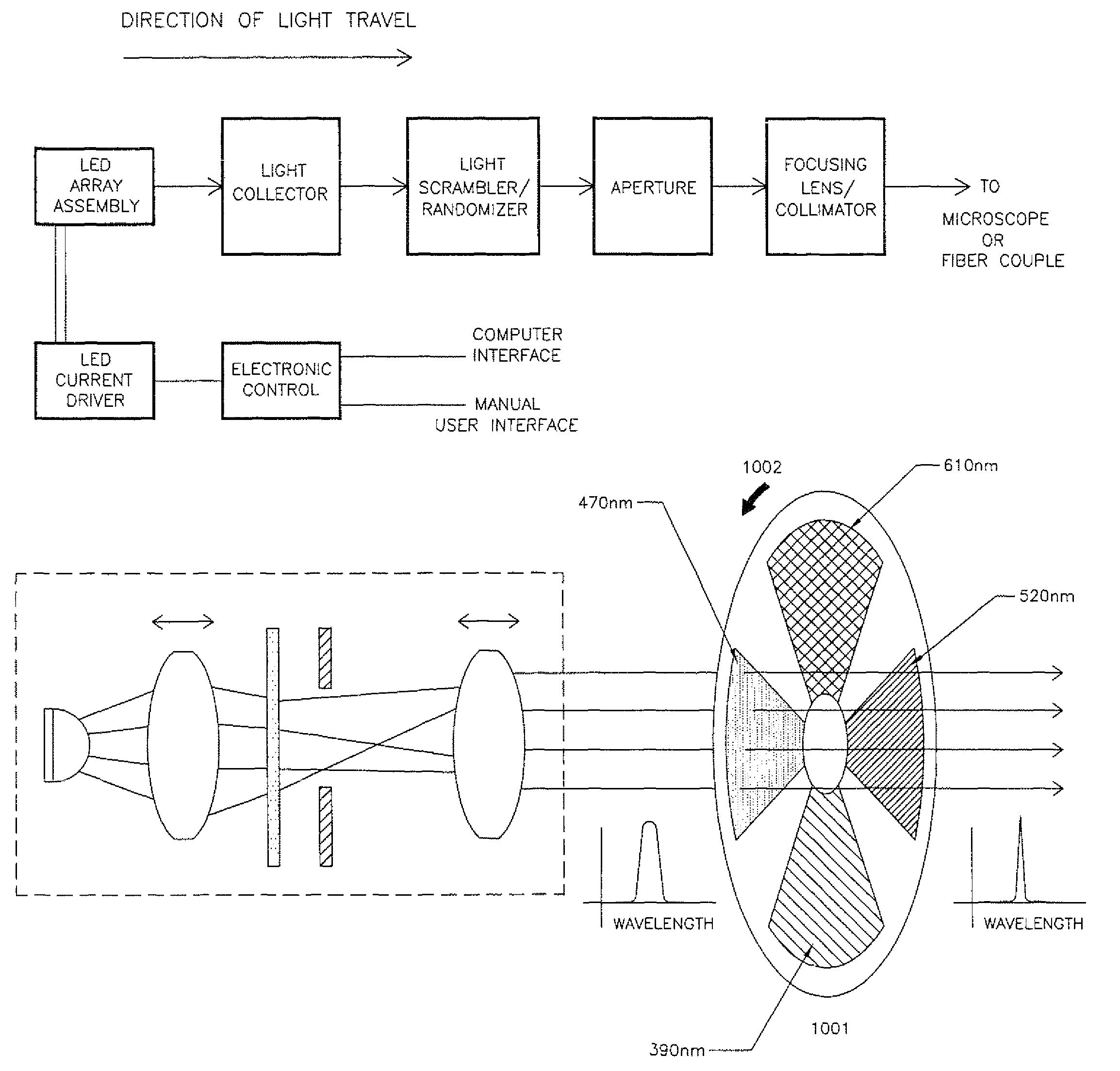
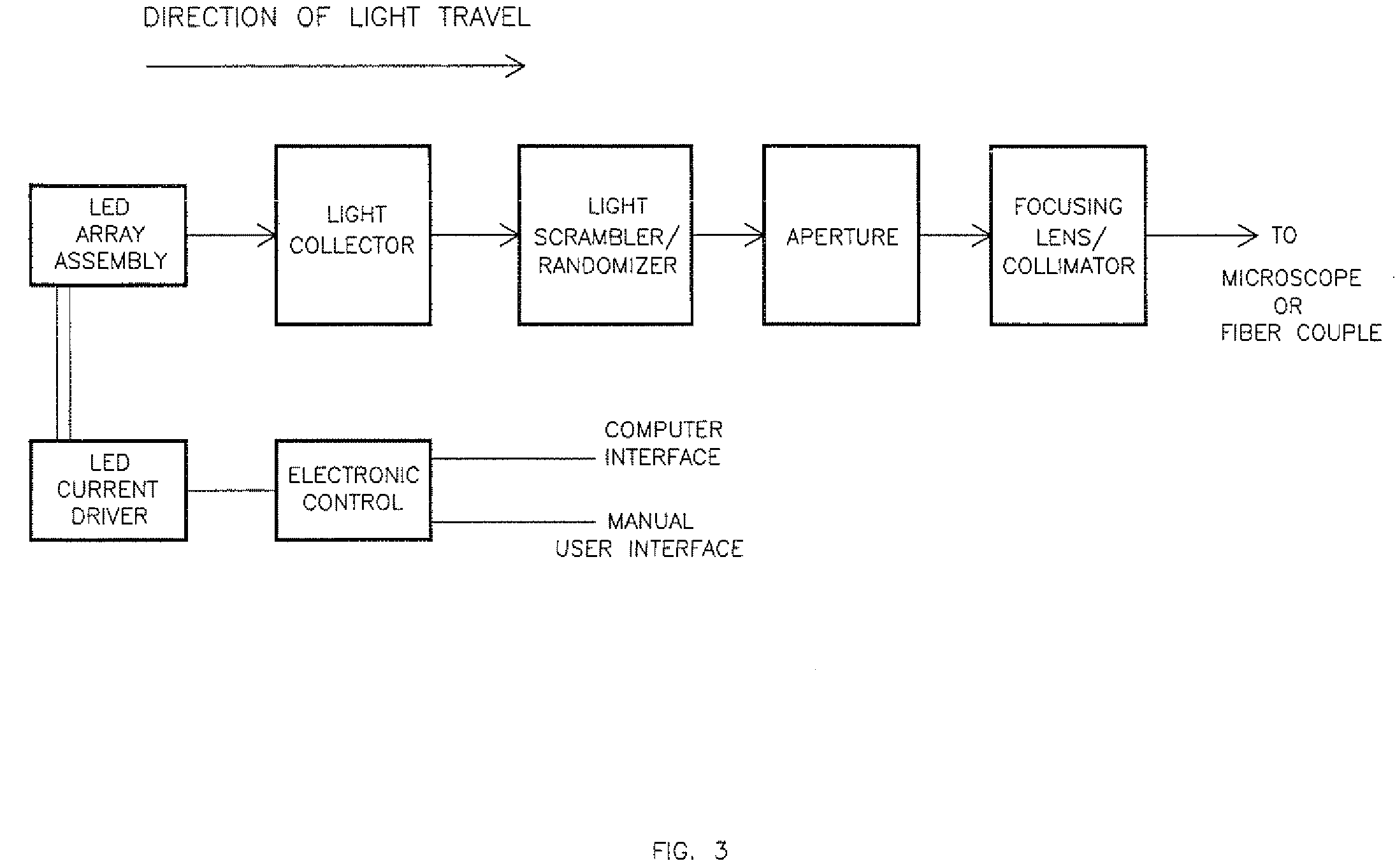
[0028]A compact multiple wavelength illuminating apparatus is disclosed herein, comprising one or more LED array with accompanying optical elements that outputs intense, spectrally narrow light uniformly over a field of view. The LED array contains multiple strings, each string comprising several LED chips of the same wavelength, where the wavelength of each string is preferably different from wavelengths of the other strings, with each string controlled electronically as a separate channel. Alternatively, each string may comprise LED chips that emit different wavelengths, where the group of wavelengths emitted by each string is different from the groups of wavelengths emitted by the other strings, and where there can be overlap between the groups of wavelengths emitted by the different strings.

[0029]Several major advantages result from the use of an LED array that contains LED chips of multiple wavelengths, organized into separately controlled strings. Multiple exciting wavelengths...


PUM


Abstract

One embodiment provides light along an optical axis. It comprises a substrate and at least one array of multiple LED chips without individual packaging supported by the substrate. The LED chips emit light within different wavelength ranges and are distributed laterally with respect to the axis over an area, the LED chips having light emitting surfaces for emitting light in directions transverse to the area. An optical element adjacent to the light emitting surfaces of the LED chips in the at least one array collects and directs light emitted by the LED chips of the at least one array along the axis towards a target. Another embodiment is directed to a method for providing multiple wavelength light for fluorescent microscopy using the above system. Electric current is supplied to the multiple LED chips, causing them to emit light of multiple wavelengths. The currents supplied to the multiple LED chips are controlled so as to control the exposure of fluorescent dyes with different excitation wavelengths wherein the light emitted by the multiple LED chips include wavelength components at such different excitation wavelengths without having to move the multiple LED chips.

Description

BACKGROUND[0001]The present invention relates generally to illumination apparatuses used for purposes such as fluorescence microscopy, and specifically to an illumination apparatus comprising a multiple wavelength light emitting diode (LED) array and its accompanying optical elements.[0002]Fluorescence microscopy is popularly used in numerous bio / medical applications since it enables users to label and observe specific structures or molecules. Briefly, fluorescence is a chemical process where when light of a specific wavelength is shined upon a fluorescent molecule, electrons are excited to a high energy state in a process known as excitation. These electrons remain briefly in this high energy state, for roughly a nanosecond, before dropping back to a low energy state and emitting light of a lower wavelength. This process is referred to as fluorescent emission, or alternatively as fluorescence.[0003]In a typical fluorescence microscopy application, one or more types of fluorescent m...

Claims


Application Information

Patent Timeline
Patent Type & Authority Patents(United States)
IPC IPC(8): G02B21/06H05B37/02F21V9/00
CPCG02B21/16F21V9/00F21K9/50G02B26/008F21K9/60
Inventor LEE, JEFFREY B.LU, JUNYING JONATHANSCHLEICHER, ROBERT E.
Owner DICON FIBEROPTICS
Why Eureka
Try Eureka