Stacked memory devices

a memory device and stacking technology, applied in the field of stacking memory devices, can solve the problems of restricted increases in integration density, difficult arrangement of circuits for supporting operations of multi-layer memory devices, etc., and achieve the effect of easy and/or high integration

Active Publication Date: 2013-12-17
SAMSUNG ELECTRONICS CO LTD
View PDF10 Cites 40 Cited by
  • Summary
  • Abstract
  • Description
  • Claims
  • Application Information

AI Technical Summary

Benefits of technology

[0007]Example embodiments may provide stacked memory devices capable of being easily and / or highly integrated.

Problems solved by technology

However, circuits for supporting operations of multilayer memory devices may not be easily arranged and / or increases in integration density may be restricted.

Method used


Image

  • Stacked memory devices
  • Stacked memory devices
  • Stacked memory devices

Examples


Embodiment Construction

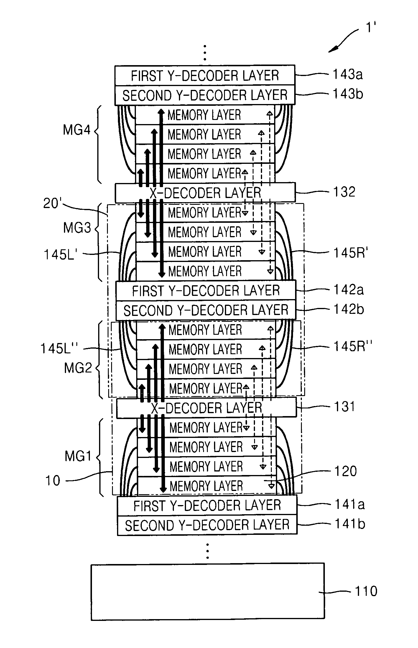
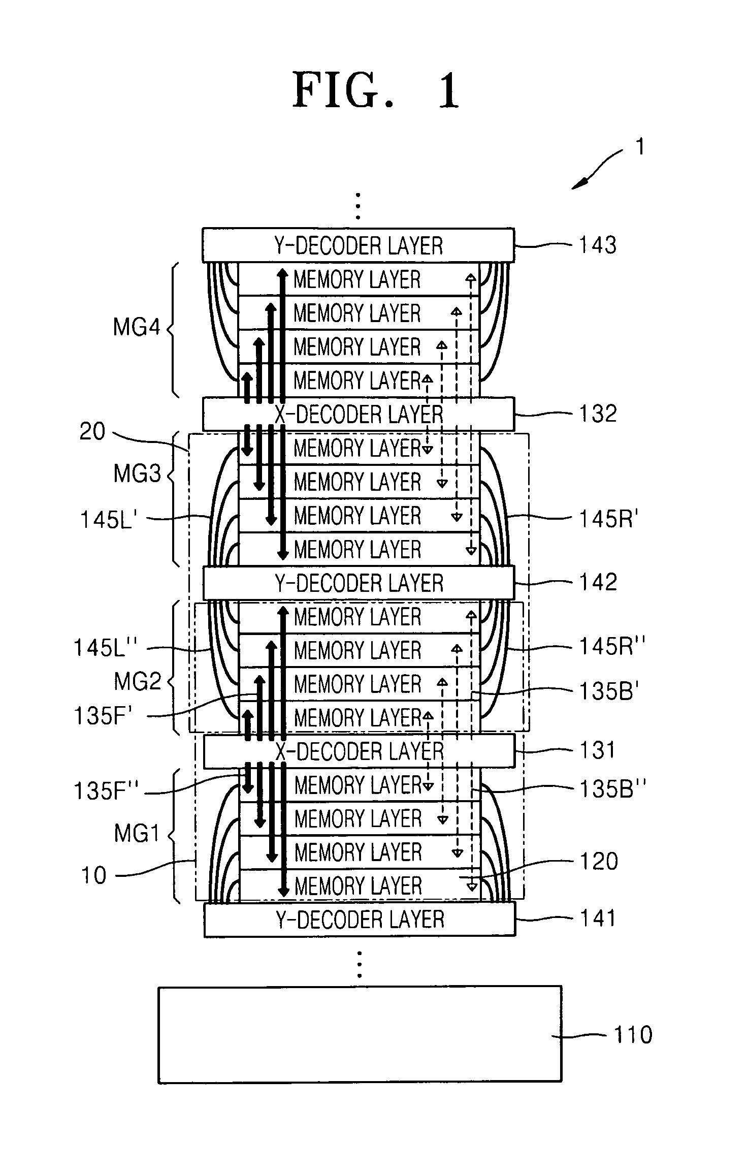
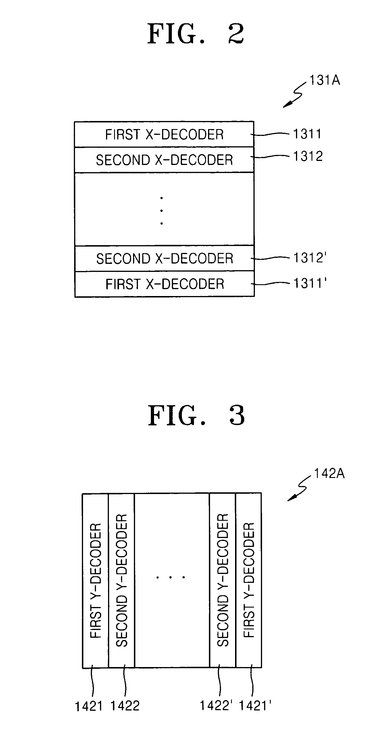
[0046]Example embodiments will now be described more fully with reference to the accompanying drawings. Embodiments, however, may be embodied in many different forms and should not be construed as being limited to the embodiments set forth herein. Rather, these example embodiments are provided so that this disclosure will be thorough and complete, and will fully convey the scope to those skilled in the art. In the drawings, the thicknesses of layers and regions are exaggerated for clarity.

[0047]It will be understood that when an element is referred to as being “on,”“connected to,”“electrically connected to,” or “coupled to” to another component, it may be directly on, connected to, electrically connected to, or coupled to the other component or intervening components may be present. In contrast, when a component is referred to as being “directly on,”“directly connected to,”“directly electrically connected to,” or “directly coupled to” another component, there are no intervening comp...


PUM


Abstract

A stacked memory device may include a substrate, a plurality of memory groups sequentially stacked on the substrate, each memory group including at least one memory layer, a plurality of X-decoder layers, at least one of the plurality of X-decoder layers being disposed between every alternate neighboring two of the plurality of memory groups, and a plurality of Y-decoder layers disposed alternately with the plurality of X-decoder layers, at least one of the plurality of Y-decoder layers being disposed between every alternate neighboring two of the plurality of memory groups.

Description

CROSS-REFERENCE TO RELATED APPLICATION(S)[0001]This application claims priority from Korean Patent Application No. 10-2009-0038949, filed on May 4, 2009, and Korean Patent Application No. 10-2010-0004481, filed on Jan. 18, 2010, in the Korean Intellectual Property Office (KIPO), the entire contents of both of which are incorporated herein by reference.BACKGROUND[0002]1. Field[0003]Example embodiments relate to semiconductor devices. Also, example embodiments relate to memory devices stacked in multilayer structures.[0004]2. Description of the Related Art[0005]As semiconductor products may be getting smaller, demand for processing large amounts of data may be increasing. As such, the need for increased integration of nonvolatile memory devices used in semiconductor products may also be increasing. In this regard, multilayer memory devices formed by stacking memory layers three-dimensionally may be considered.[0006]However, circuits for supporting operations of multilayer memory devic...

Claims


Application Information

Patent Timeline
Patent Type & Authority Patents(United States)
IPC IPC(8): G11C5/02
CPCG11C5/02G11C5/025G11C8/10G11C13/0023G11C13/0028G11C13/0004G11C2213/72G11C2213/71
Inventor AHN, SEUNG-EONKIM, HO-JUNGPARK, CHUL-WOOKANG, SANG-BEOMCHOI, HYUN-HO
Owner SAMSUNG ELECTRONICS CO LTD
Why Eureka
Try Eureka