Lead frame and its chip package

A technology of chip packaging and lead frame, which is applied in the direction of semiconductor devices, semiconductor/solid-state device parts, electric solid-state devices, etc., to achieve the effects of saving PCB space, facilitating high circuit integration, and simple process

Active Publication Date: 2018-04-17
GREAT TEAM BACKEND FOUNDRY (DONGGUAN) LTD
View PDF4 Cites 1 Cited by
  • Summary
  • Abstract
  • Description
  • Claims
  • Application Information

AI Technical Summary

Problems solved by technology

Simplify the packaging process

Method used


Image

  • Lead frame and its chip package
  • Lead frame and its chip package
  • Lead frame and its chip package

Examples


Embodiment 1

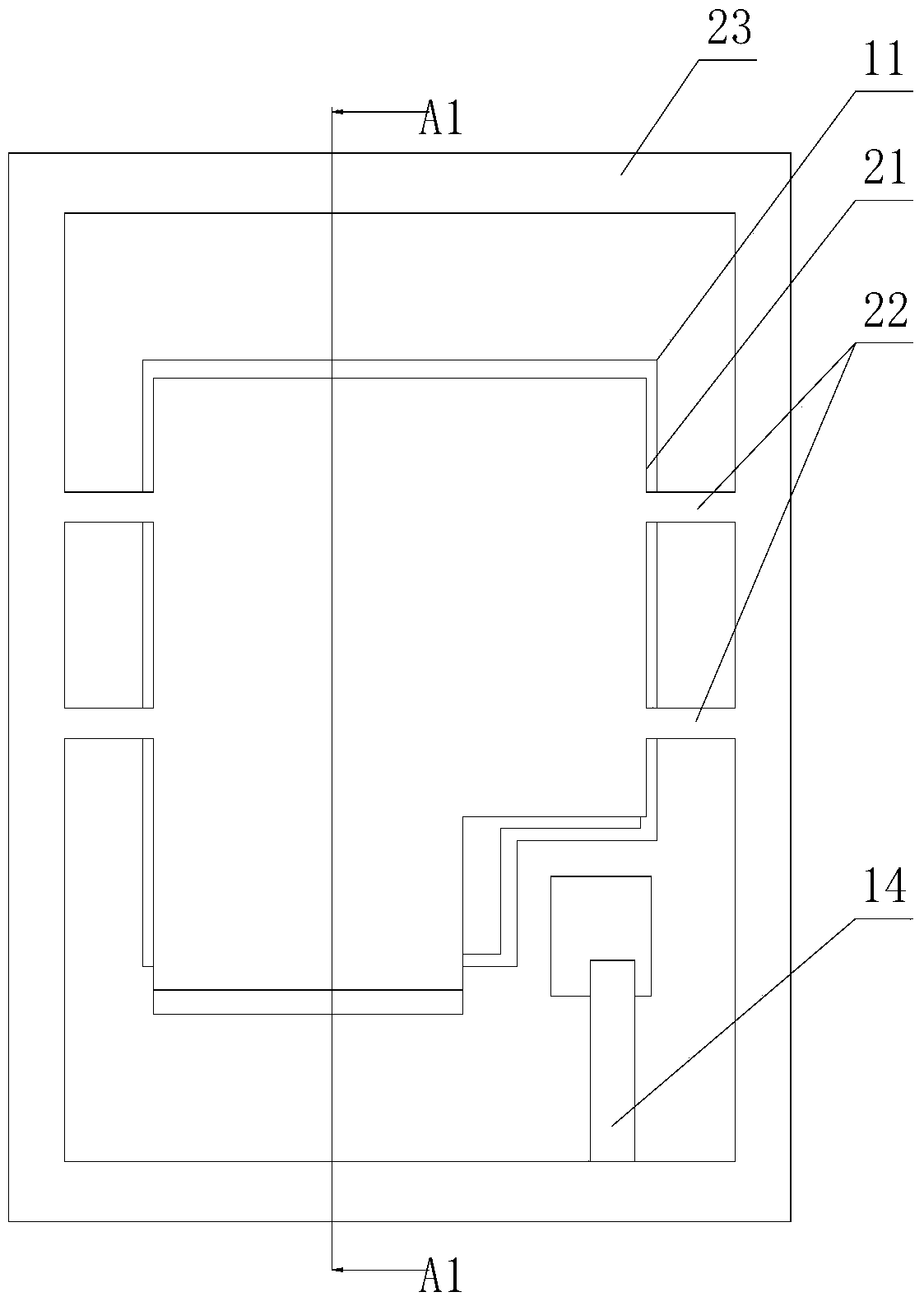
[0043] refer to Figure 1 to Figure 6 , the lead frame provided in Embodiment 1 of the present invention includes a first lead frame and a bridge frame,

[0044] The first lead frame includes a first chip holder 11, a plurality of first connecting rods 12, a first outer pin 14 and a first outer frame 13, the outer end of the first connecting rod 12 is connected to the first Outer frame 13 is connected, and its inner end is connected with described first chip seat 11, and the outer end of described first external pin 14 is connected with described first outer frame 13, and its inner end is placed on described first chip. The gate of the chip on seat 11 is turned on,

[0045] The bridge frame includes a second chip holder 21, a plurality of second connecting rods 22 and a second outer frame 23, the outer ends of the second connecting rods 22 are connected to the second outer frame 23, and the inner ends thereof are connected to the second outer frame 23. The second chip holder...

Embodiment 2

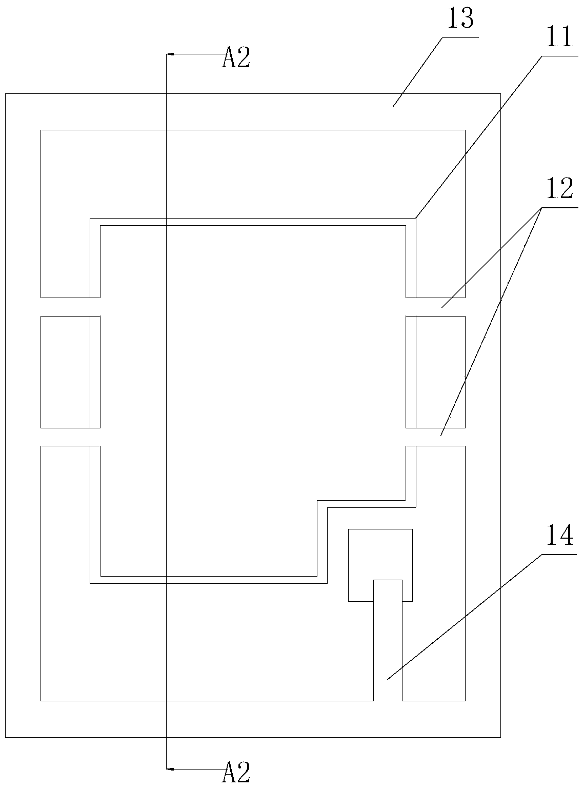
[0051] refer to Figure 7 to Figure 10 , the chip package provided by Embodiment 2 of the present invention includes:

[0052] The first lead frame, the first lead frame includes a first chip holder 11, a first external pin 14 and a plurality of first connecting rods 12, the inner ends of the first connecting rods 12 are connected to the first chip holder 11 connection, the inner end of the first external pin 14 is conducted with the gate of the flip chip placed on the first chip holder 11;

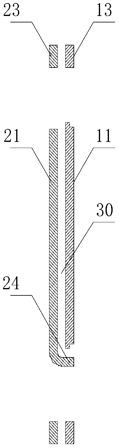
[0053] A bridge frame, the bridge frame is superimposed on the first lead frame, the bridge frame includes a second chip holder 21, a plurality of second connecting rods 22, the inner ends of the second connecting rods 22 are connected to the The second chip holder 21 is connected, the bottom of the second chip holder 21 is provided with a folded edge 24, the bottom of the folded edge 24 is on the same level as the lower surface of the first chip holder 11, and the first chip A space 30...

Embodiment 3

[0060] refer to Figure 11 to Figure 14 The main difference between the chip package provided by Embodiment 3 of the present invention and the chip package provided by Embodiment 2 is that the upper surface of the bridge frame leaks outside the encapsulant 50 . Other structures are the same as those in Embodiment 2.


PUM


Abstract

The invention discloses a lead frame, including a first lead frame and a bridge frame, the first lead frame includes a first chip seat, a plurality of first connecting rods, a first external pin and a first outer frame, the first lead frame The outer end of a connecting rod is connected with the first outer frame, the inner end is connected with the first chip holder, the outer end of the first outer pin is connected with the first outer frame, and the inner end is connected with the first outer frame. The gate of the chip placed on the first chip holder is turned on, and the bridge frame includes a second chip holder, a plurality of second connecting rods and a second outer frame, and the outer ends of the second connecting rods are connected to the second outer frame. The second outer frame is connected, and its inner end is connected to the second chip holder, and the lower side of the second chip holder is provided with a folded edge. When the bridge frame is stacked on the top of the first lead frame, the The bottom of the folded edge is on the same level as the lower surface of the first chip holder, and a space for bonding chips is provided between the first chip holder and the second chip holder.

Description

technical field [0001] The invention relates to the technical field of semiconductor packaging, in particular to a lead frame and a chip packaging body thereof. Background technique [0002] The semiconductor device packaging method is to arrange the chip cut from the wafer on the lead frame and electrically connect the chip to the lead frame, and then cover the chip with the encapsulation gel to prevent the chip from being damaged by the harsh external environment and provide The medium for the electrical connection between the chip and the external circuit. [0003] The current packaging method is to bond the chip on the chip holder of the lead frame through a bonding material, and then electrically connect the chip and the pins by welding gold wires. Due to the existence of the welding wires, the packaging area is large and the packaging volume is large. , the packaging process is complex. Contents of the invention [0004] The object of the present invention is to pr...

Claims


Application Information

Patent Timeline
Patent Type & Authority Patents(China)
IPC IPC(8): H01L23/495H01L23/49
CPCH01L2924/181H01L2924/00014H01L2224/84801H01L24/84H01L24/40H01L2924/00012H01L2224/37099H01L2224/37599H01L2224/34H01L2224/83801
Inventor 曹周徐振杰
Owner GREAT TEAM BACKEND FOUNDRY (DONGGUAN) LTD
Why Eureka
Try Eureka