Liquid crystal display device, manufacturing method of liquid crystal display device, display device and information input apparatus

a technology of liquid crystal display device and manufacturing method, which is applied in the manufacture of electrode systems, electric discharge tubes/lamps, instruments, etc., can solve the problems of reducing yield, increasing manufacture costs, and deteriorating manufacturing efficiency, so as to reduce manufacturing costs, improve yield, and improve manufacturing efficiency

Active Publication Date: 2014-01-07
JAPAN DISPLAY WEST
View PDF10 Cites 58 Cited by
  • Summary
  • Abstract
  • Description
  • Claims
  • Application Information

AI Technical Summary

Benefits of technology

[0015]Besides, since it is difficult to sufficiently remove the liquid crystal orientation film from the surface portion of the touch electrode, yield can decrease.
[0017]Further, in the above method, since there is a case where the periphery of an area where the surface is exposed is also dissolved, it is necessary to provide a margin. Thus, in the liquid crystal panel, a portion occupied by the touch sensor is increased, and the aperture ratio of the liquid crystal panel can decrease. Thus, the brightness of a display image is reduced and the image quality can deteriorate.
[0020]In order to resolve such a problem, the surface of the convex part on which the touch electrode is provided may increase in area. In this case, however, the aperture ratio of the liquid crystal panel decreases, which may cause deterioration in quality of a display image.
[0022]Thus, it is desirable to provide a liquid crystal display device, a manufacturing method of a liquid crystal display device, a display device and an information input device, in which manufacture efficiency, yield and image quality can be improved, and manufacture cost can be reduced.
[0032]According to the embodiments of the invention, the liquid crystal display device, the manufacturing method of the liquid crystal display device, the display device, and the information input device can be provided in which the manufacture efficiency, yield, and image quality can be improved and the manufacture cost can be reduced.

Problems solved by technology

However, in the above method, since it is difficult to obtain a sufficient throughput, the manufacture efficiency can deteriorate.
Besides, since it is difficult to sufficiently remove the liquid crystal orientation film from the surface portion of the touch electrode, yield can decrease.
Besides, since it is necessary to newly introduce the above instrument, the manufacture cost can increase.

Method used


Image

  • Liquid crystal display device, manufacturing method of liquid crystal display device, display device and information input apparatus
  • Liquid crystal display device, manufacturing method of liquid crystal display device, display device and information input apparatus
  • Liquid crystal display device, manufacturing method of liquid crystal display device, display device and information input apparatus

Examples


embodiment 1

(Structure of Liquid Crystal Display Device)

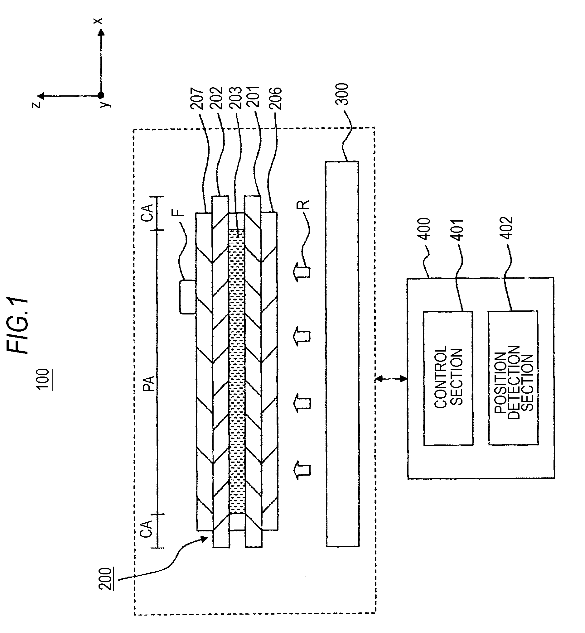
[0100]FIG. 1 is a sectional view showing a structure of a liquid crystal display device 100 of Embodiment 1 of the invention.

[0101]As shown in FIG. 1, the liquid crystal display device 100 of this embodiment includes a liquid crystal panel 200, a backlight 300, and a data processing section 400. The respective parts will be described in sequence.

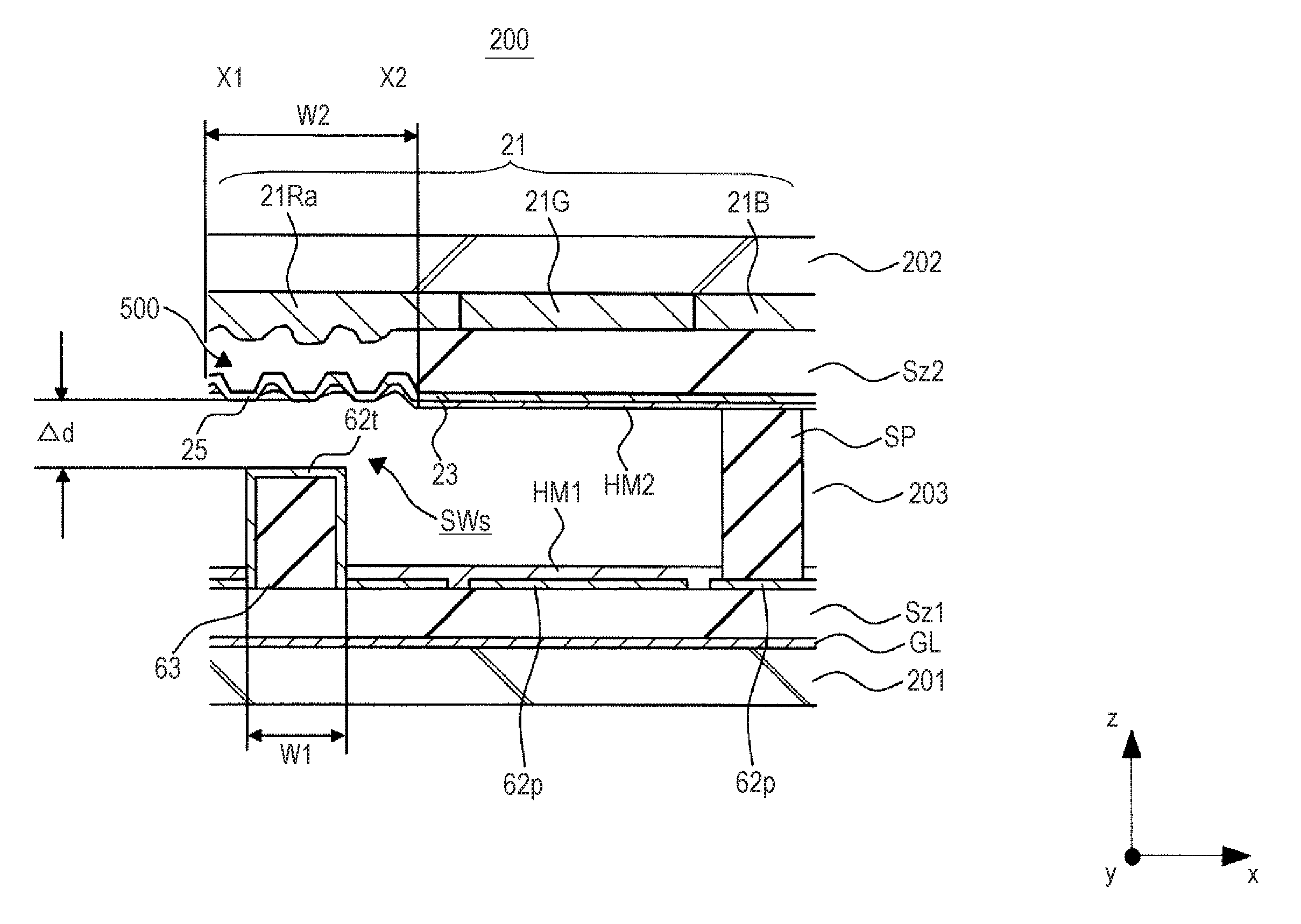
[0102]For example, the liquid crystal panel 200 is of an active matrix type, and includes, as shown in FIG. 1, a TFT array substrate 201, an opposite substrate 202 and a liquid crystal layer 203. In the liquid crystal panel 200, the TFT array substrate 201 and the opposite substrate 202 are spaced from and opposite to each other. The liquid crystal layer 203 is provided to be sandwiched between the TFT array substrate 201 and the opposite substrate 202.

[0103]As shown in FIG. 1, in the liquid crystal panel 200, a first polarizing plate 206 is disposed on a surface of the TFT array substrate 201 oppo...

embodiment 2

[0214]Hereinafter, Embodiment 2 of the invention will be described.

(Detailed Structure of Liquid Crystal Panel)

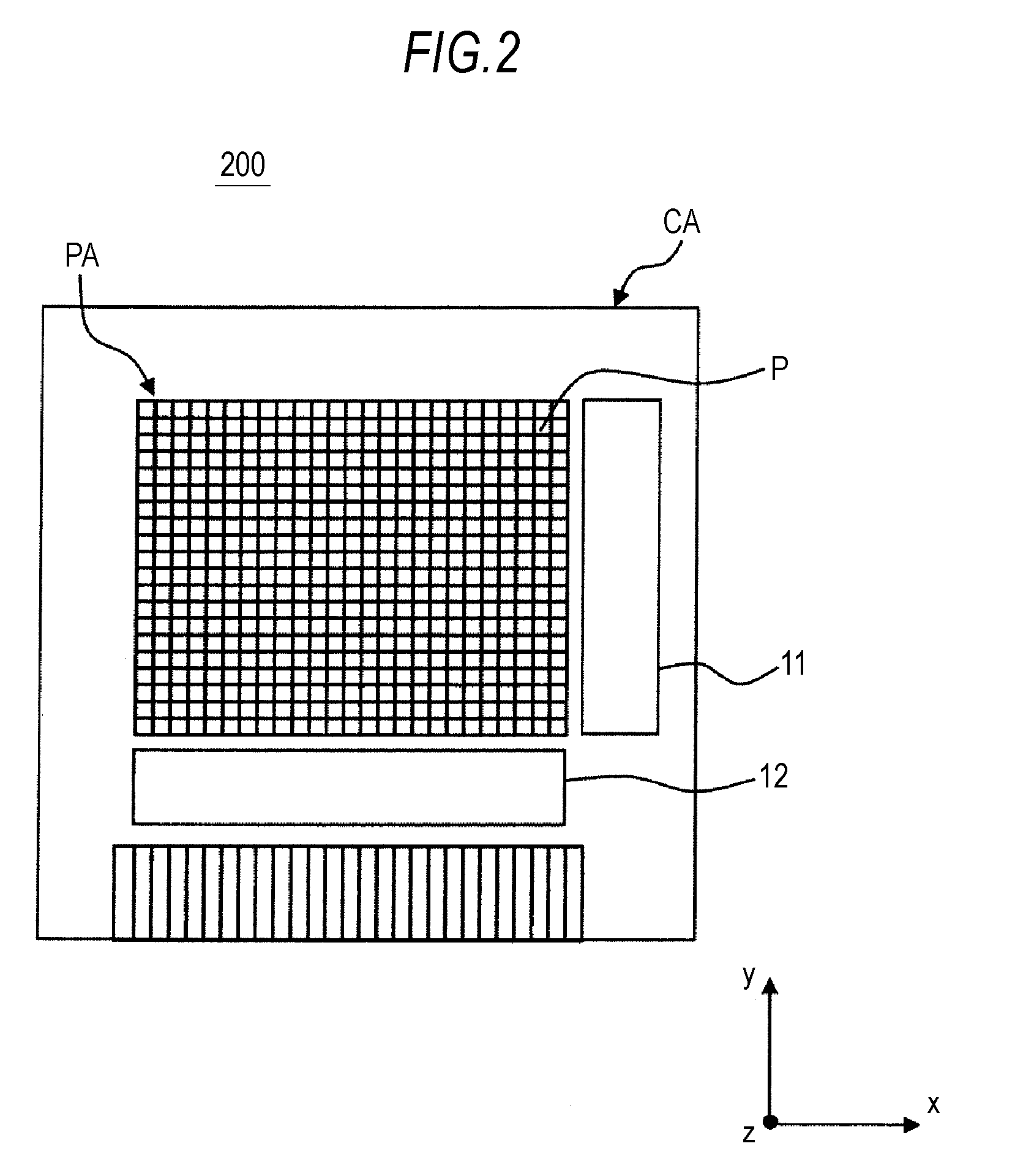
[0215]FIG. 15 is a view showing the main part of a liquid crystal panel 200b of Embodiment 2 of the invention. Here, FIG. 15 is a sectional view schematically showing the outline of a pixel P provided in a display area PA of a liquid crystal panel 200b of Embodiment 2 of the invention.

[0216]As shown in FIG. 15, in this embodiment, a structure of a touch sensor switch SWsb is different from that of Embodiment 1. Specifically, as is understood by comparing FIG. 15 with FIG. 3, a touch electrode 25b formed on an opposite substrate 202 is different from that of Embodiment 1. Besides, a touch electrode 62tb formed on a TFT array substrate 201 is different from that of Embodiment 1. This embodiment is similar to Embodiment 1 except for this point and points relevant thereto. Thus, the description of duplicate portions is omitted.

[0217]In the opposite substrate 202, as shown in FI...

embodiment 3

[0230]Hereinafter, Embodiment 3 of the invention will be described.

(Detailed Structure of Liquid Crystal Panel)

[0231]FIG. 17 is view showing a main part of a liquid crystal panel 200c of Embodiment 3 of the invention. Here, FIG. 17 is a sectional view schematically showing the outline of a pixel P provided in a display area PA in the liquid crystal panel 200c of this embodiment.

[0232]As shown in FIG. 17, in this embodiment, a structure of a touch sensor switch SWsc is different from that of Embodiment 1. Specifically, as is understood by comparing FIG. 17 with FIG. 3, a portion of a touch electrode 25c formed on an opposite substrate 202 is different from that of Embodiment 1. This embodiment is similar to Embodiment 1 except for this point and points relevant thereto. Thus, the description of duplicate portions is omitted.

[0233]As shown in FIG. 17, the touch electrode 25c is provided on the opposite substrate 202 so as to cover the surface of a concave and convex area 500c.

[0234]I...


PUM


Abstract

A display device includes: a display panel including first and second substrates spaced from and opposite to each other, and has a touch sensor switch. The touch sensor switch includes a first touch electrode provided on a surface of the first substrate facing the second substrate, and a second touch electrode provided on a surface of the second substrate facing the first substrate and spaced from and faces the first touch electrode. The first and second touch electrodes contact with each other when the touch panel is deformed by an external pressure. The first touch electrode covers a surface of a concave and convex area where grooves are formed to be spaced from each other, and on the surface on which the first touch electrode is provided, an application film is provided to expose a surface of a top face of a convex part of the concave and convex area.

Description

BACKGROUND OF THE INVENTION[0001]1. Field of the Invention[0002]The present invention relates to a liquid crystal display device, a manufacturing method of a liquid crystal display device, a display device and an information input apparatus. Particularly, the invention relates to a liquid crystal display device, a manufacturing method of a liquid crystal display device, a display device and an information input apparatus, in which a touch sensor switch is provided on a pair of substrates opposite to each other.[0003]2. Description of the Related Art[0004]A display device, such as a liquid crystal display device or an organic EL display device, has merits such as low thickness, lightweight and low power consumption. Thus, the display device is often used in a mobile electronic equipment, such as a cellular phone or a digital camera.[0005]In the display device as stated above, the liquid crystal display device includes, as a display panel, a liquid crystal panel in which a liquid crys...

Claims


Application Information

Patent Timeline
Patent Type & Authority Patents(United States)
IPC IPC(8): G06F3/041
CPCG06F3/0412G02F1/13338G06F3/047G02F2001/134372G02F1/134363G02F2201/40G02F1/1337G02F1/13394G02F1/134372
Inventor TAMAKI, MASAYAKOITO, TAKEOIMAI, MASATO
Owner JAPAN DISPLAY WEST
Why Eureka
Try Eureka