Background selection of voltage reference values for performing memory read operations

a technology of voltage reference value and memory read operation, which is applied in the direction of digital storage, error detection/correction, instruments, etc., can solve the problems of device wear caused by usage, read operation failure, and charge loss or leakag

Active Publication Date: 2014-01-28
WESTERN DIGITAL TECH INC
View PDF18 Cites 205 Cited by
  • Summary
  • Abstract
  • Description
  • Claims
  • Application Information

AI Technical Summary

Problems solved by technology

Various factors can contribute to data read errors in flash memory devices.
These factors include charge loss or leakage over time, and device wear caused by usage.
When the number of bit errors on a read operation exceeds the ECC (error correction code) correction capability of the storage subsystem, the read ope

Method used


Image

  • Background selection of voltage reference values for performing memory read operations
  • Background selection of voltage reference values for performing memory read operations
  • Background selection of voltage reference values for performing memory read operations

Examples


Embodiment Construction

[0012]Specific embodiments of a storage system and an associated voltage reference testing process will now be described with reference to the drawings. This description is intended to illustrate specific embodiments of the invention, and is not intended to be limiting. Thus, nothing in this description is intended to imply that any particular component, step or characteristic is essential. The invention is defined only by the claims.

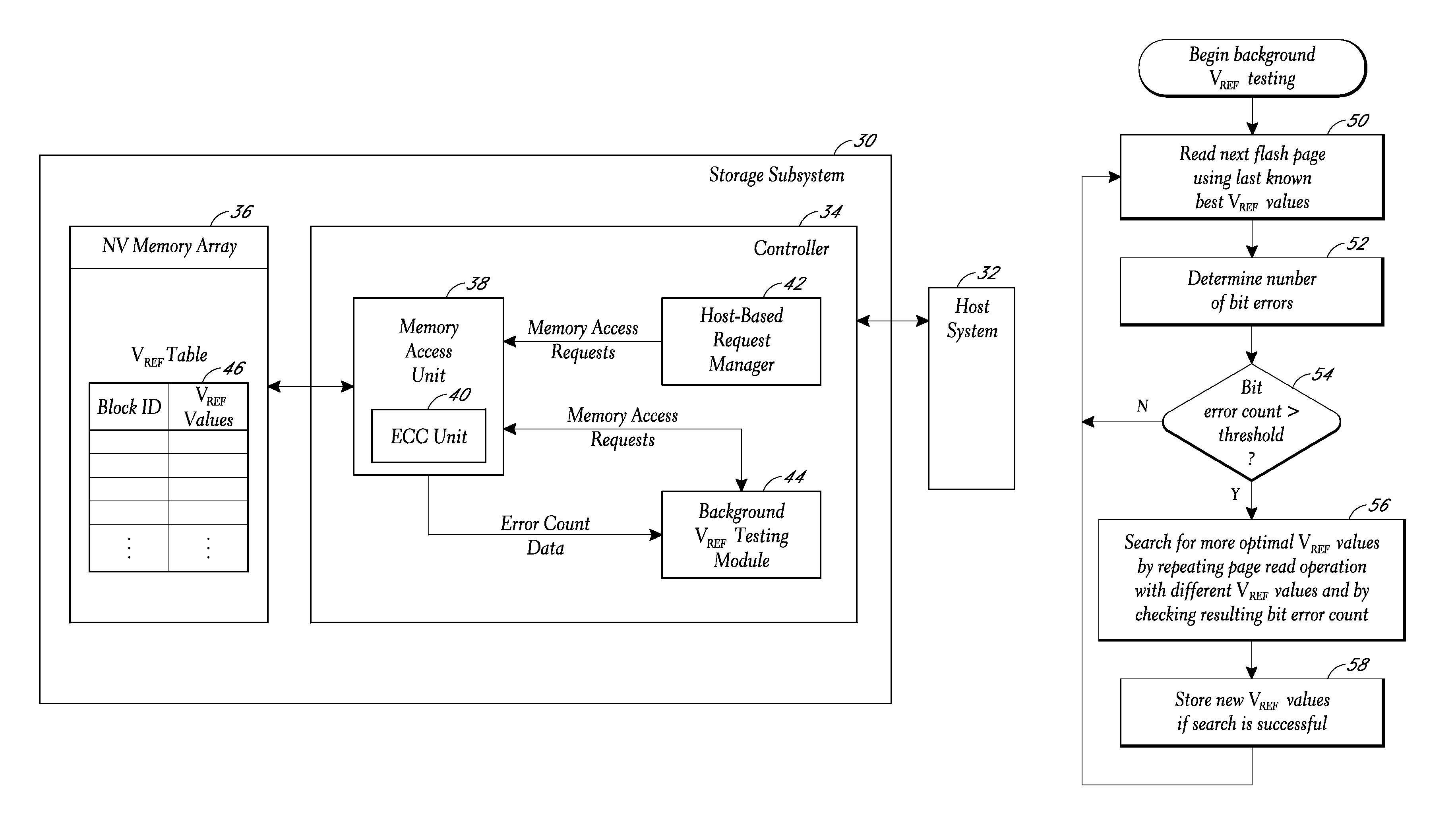
[0013]FIG. 1 illustrates a storage subsystem 30 that implements a background voltage reference (Vref) testing process according to one embodiment. The storage subsystem 30 is shown connected to a host system 32 that writes and reads data to / from the storage subsystem 30. The storage subsystem 30 may implement an ATA command set and interface, although other command sets and interfaces may additionally or alternatively be used.

[0014]The storage subsystem 30 includes a controller 34 that accesses an array of non-volatile (NV) solid state memory 36. The co...


PUM


Abstract

A storage subsystem implements a background process for selecting voltage reference values to use for reading data from a non-volatile memory array, such as an array of multi-level cell (MLC) flash memory. The process involves performing background read operations using specific sets of voltage reference values while monitoring the resulting bit error counts. The selected voltage reference values for specific pages or other blocks of the array are stored in a table. Read operations requested by a host system are executed using the corresponding voltage reference values specified by the table.

Description

CROSS-REFERENCE TO RELATED APPLICATIONS[0001]The present application claims priority from co-pending provisional U.S. Patent Application Ser. No. 61 / 381,913, filed on Sep. 10, 2010, the specification of which is incorporated herein by reference.BACKGROUND[0002]1. Technical Field[0003]This disclosure relates to solid state memory devices that use voltage reference values to determine the states of memory cells. More particularly, the disclosure relates to processes for selecting voltage reference values to use for performing memory read operations.[0004]2. Description of the Related Art[0005]Flash memory devices store information in an array of memory cells constructed with floating gate transistors. In single-level cell (SLC) flash devices, each cell stores a single bit of information. In multi-level cell (MLC) devices, each cell stores two or more bits of information. When a read operation is performed, the electrical charge levels of the cells are compared to one or more voltage r...

Claims


Application Information

Patent Timeline
IPC IPC(8): G11C11/34
CPCG11C2029/0409G11C5/147G11C16/3422G11C16/30G06F11/1072G11C29/028G11C29/021G11C11/34G06F11/1068G11C29/50004G11C2029/4402
Inventor HORN, ROBERT, L.
Owner WESTERN DIGITAL TECH INC
Why Eureka
Try Eureka