Photoelectric conversion device

a conversion device and photoelectric technology, applied in the direction of energy conversion device, semiconductor device, electrical apparatus, etc., can solve the problems of reducing the diffusion length of minority carriers (electrons) generated reducing being susceptible to defects present in the light-absorbing layer. , to achieve the effect of improving the photoelectric conversion efficiency, reducing the occurrence of recombination, and reducing the diffusion length

Inactive Publication Date: 2014-02-18
KYOCERA CORP
View PDF20 Cites 13 Cited by
  • Summary
  • Abstract
  • Description
  • Claims
  • Application Information

AI Technical Summary

Benefits of technology

[0004]An object of the present invention is to reduce the occurrence of recombination of minority carriers due to defects in a light-absorbing layer, to thereby improve photoelectric conversion efficiency.
[0006]According to the photoelectric conversion device of the embodiment of the present invention, even if defects are generated in a part located on the electrode side of the light-absorbing layer, the defects are more likely to be filled with oxygen. Accordingly, the diffusion length of minority carriers generated in that part increases, which enables to reduce the occurrence of recombination of carriers. This results in improvement of photoelectric conversion efficiency.

Problems solved by technology

In those photoelectric conversion devices, the diffusion length of minority carriers (electrons) generated in the light-absorbing layer is reduced due to a large number of defects present in a light-absorbing layer.
In particular, the minority carriers generated in the light-absorbing layer on the backside electrode side have to be diffused over a long length, and thus are susceptible to the defects present in the light-absorbing layer.
This may lead to a decrease in photoelectric conversion efficiency.

Method used


Image

  • Photoelectric conversion device
  • Photoelectric conversion device
  • Photoelectric conversion device

Examples


Embodiment Construction

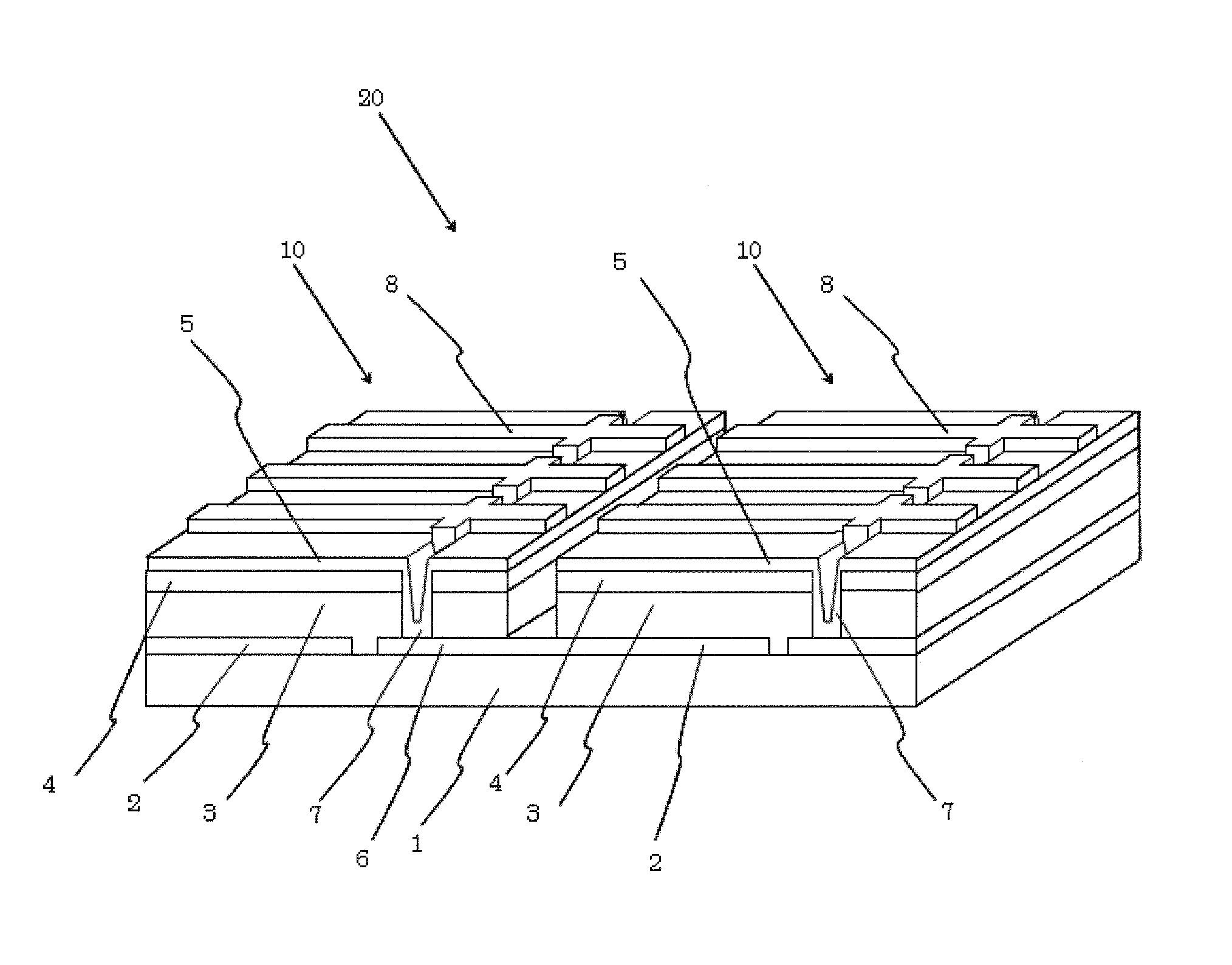
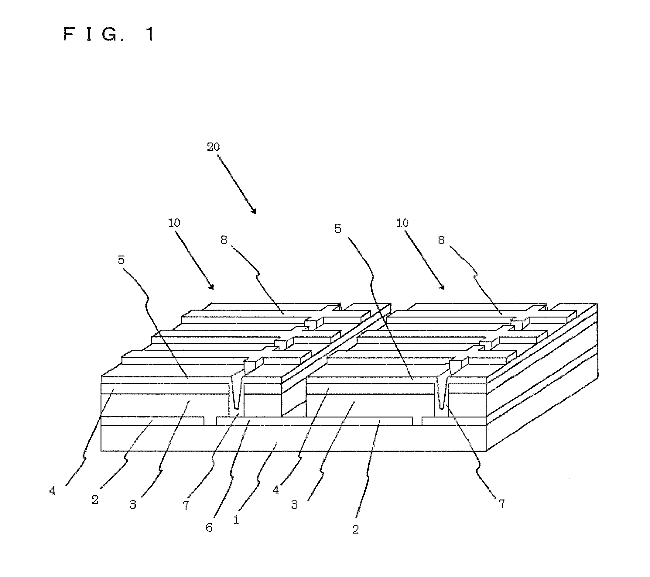
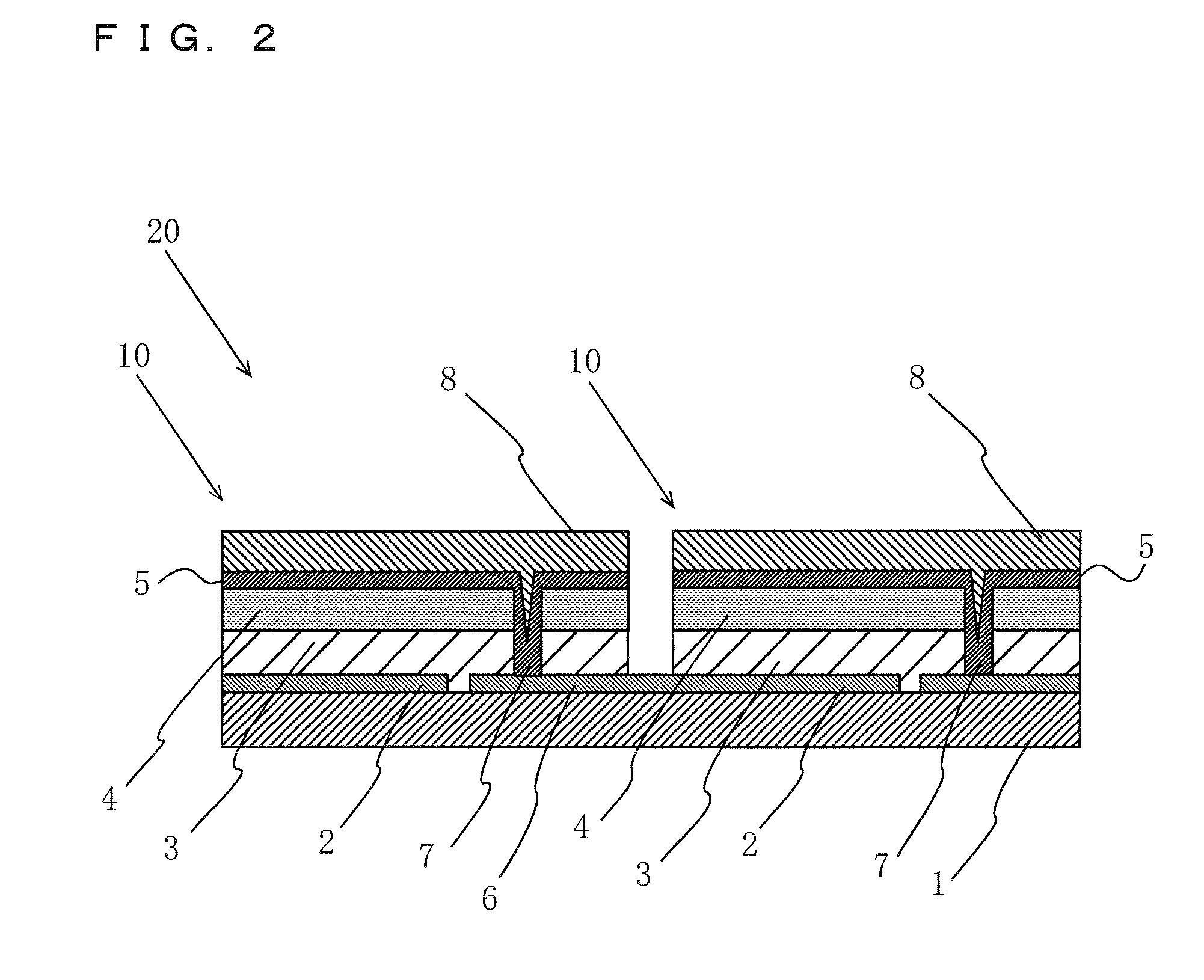
[0010]As shown in FIGS. 1 and 2, a photoelectric conversion device 10 according to an embodiment of the present invention includes a substrate 1, a first electrode layer 2, a first semiconductor layer 3, a second semiconductor layer 4, and a second electrode layer 5. The photoelectric conversion device 10 includes a third electrode layer 6 spaced apart from the first electrode layer 2 and located on the substrate 1 side of the first semiconductor layer 3. The neighboring photoelectric conversion devices 10 are electrically connected to each other by a connection conductor 7. That is, the second electrode layer 5 of one photoelectric conversion device 10 and the third electrode layer 6 of the other photoelectric conversion device 10 are connected by the connection conductor 7. The third electrode layer 6 also serves as the first electrode layer 2 of the neighboring photoelectric conversion device 10. As a result, the neighboring photoelectric conversion devices 10 are connected to ea...


PUM


Abstract

It is aimed to provide a photoelectric conversion device having high adhesion between a first semiconductor layer and an electrode layer as well as high photoelectric conversion efficiency. A photoelectric conversion device comprises an electrode layer, a first semiconductor layer located on the electrode layer and comprising a chalcopyrite-based compound semiconductor of group I-III-VI and oxygen, and a second semiconductor layer located on the first semiconductor layer and forming a pn junction with the first semiconductor layer. In the photoelectric conversion device, the first semiconductor layer has a higher molar concentration of oxygen in a part located on the electrode layer side with respect to a center portion in a lamination direction of the first semiconductor layer than a molar concentration of oxygen in the whole of the first semiconductor layer.

Description

TECHNICAL FIELD[0001]The present invention relates to a photoelectric conversion device.BACKGROUND ART[0002]As photoelectric conversion devices, there are devices including a light-absorbing layer comprised of a chalcopyrite-based group I-III-VI compound semiconductor such as CIGS. Japanese Patent Application Laid-Open No. 2000-156517 discloses an example in which a light-absorbing layer comprised of a group I-III-VI compound semiconductor is provided on a backside electrode formed on a substrate. A buffer layer comprised of ZnS, CdS, or the like and a transparent conductive film comprised of ZnO or the like are formed on the light-absorbing layer.[0003]In those photoelectric conversion devices, the diffusion length of minority carriers (electrons) generated in the light-absorbing layer is reduced due to a large number of defects present in a light-absorbing layer. As a result, in some cases, the minority carriers disappear due to the recombination with holes before being extracted ...

Claims


Application Information

Patent Timeline
Patent Type & Authority Patents(United States)
IPC IPC(8): H01L31/0272H01L31/032
CPCH01L31/0322H01L27/1423H01L31/0272Y02E10/541H01L31/0749H01L31/046
Inventor KAMADA, RUIKASAI, SHUICHI
Owner KYOCERA CORP
Why Eureka
Try Eureka