Spare cell insertion based on reachable state analysis

a technology of reachable state and spare cells, applied in the direction of instruments, computing, electric digital data processing, etc., can solve the problems of large number of cells, difficult physical design without the aid of computers, and complicated connections between cells

a technology of reachable state and spare cells, applied in the direction of instruments, computing, electric digital data processing, etc., can solve the problems of large number of cells, difficult physical design without the aid of computers, and complicated connections between cells

US8661391B1Inactive Publication Date: 2014-02-25GLOBALFOUNDRIES US INC

Image

  • Spare cell insertion based on reachable state analysis
  • Spare cell insertion based on reachable state analysis
  • Spare cell insertion based on reachable state analysis

Examples


Embodiment Construction

)

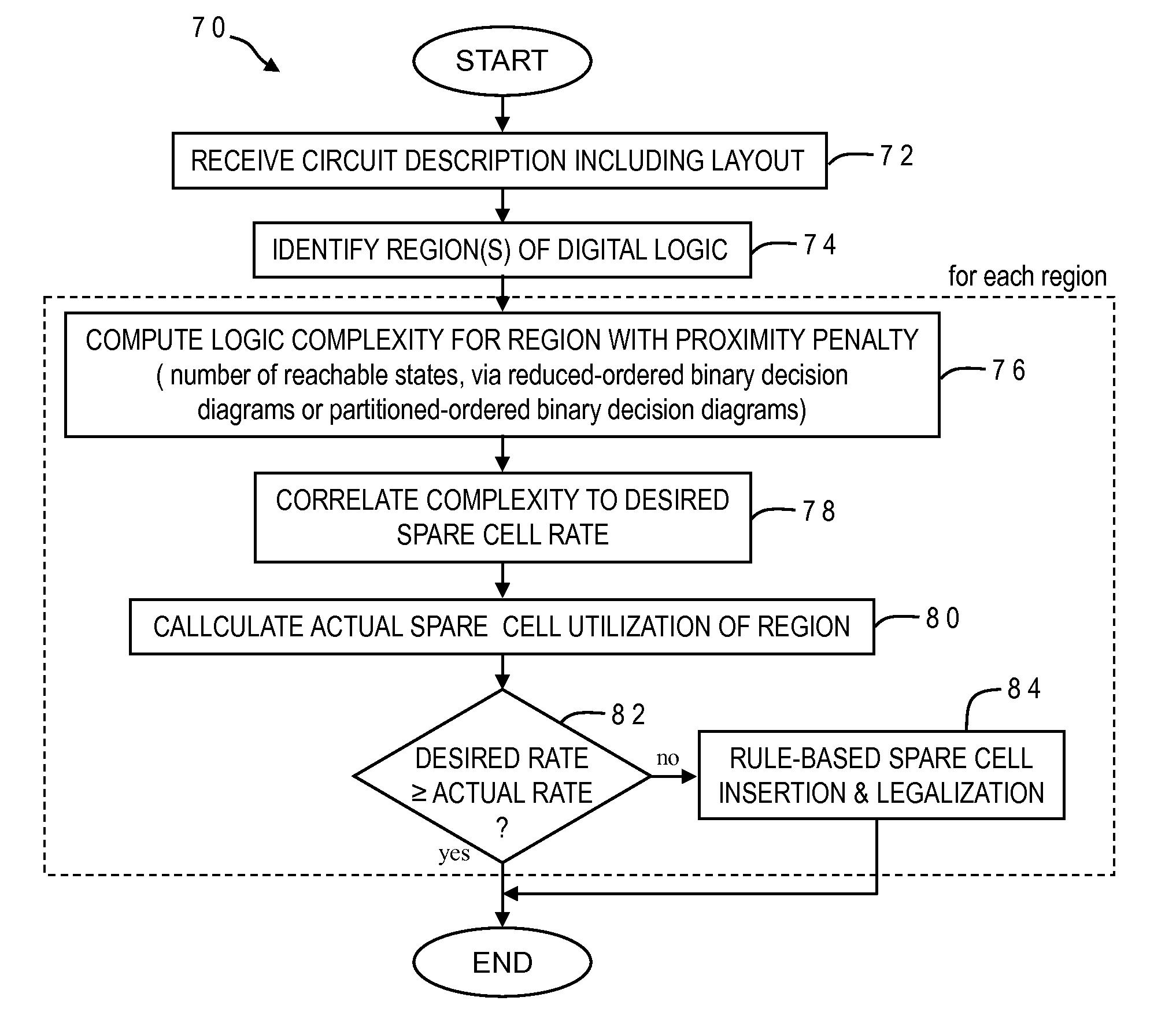
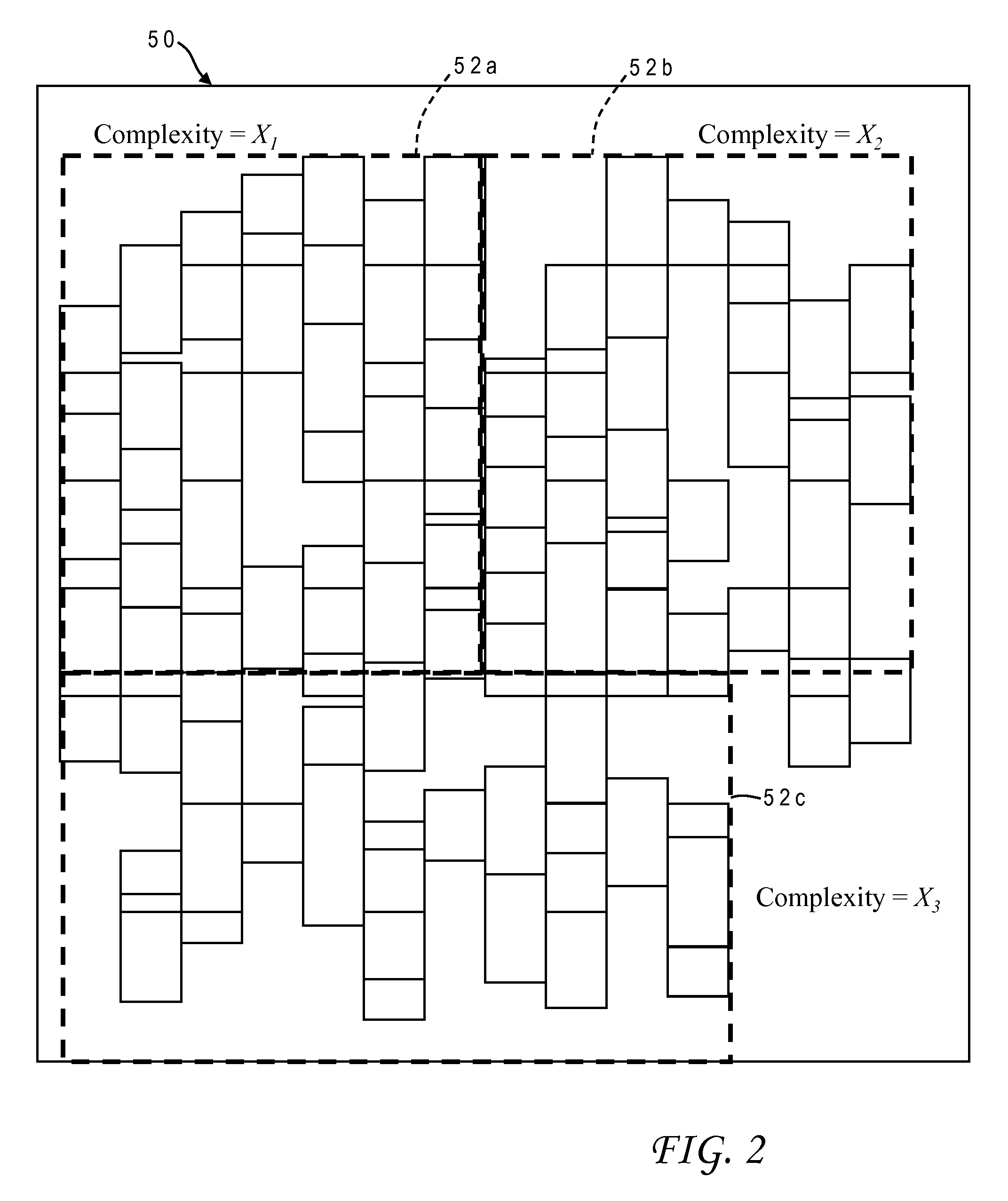
[0018]The use of spare cells greatly simplifies implementation of ECOs but there can still be problems with the locations of these cells. Since the filler percentage is applied globally to an entire design, some areas of the circuit which are more stable can end up getting too many filler cells, while other areas do not get enough. Furthermore, typical placement tools can push filler cells away from the most critical logic (which is often unstable) so even if there are filler cells available, they may not be located close enough to be of use for timing / logic fixes. Placement tools that partition the logic into separate bins can experience additional stability issues whenever the bin sizes or locations change.

[0019]Placement tools (particularly those which attempt to minimize wire length using quadratic placement) naturally pull connected logic together very tightly. This logic clustering effect can be countered by introducing a spreading factor to artificially increase instance siz...


PUM


Abstract

Spare cells are inserted in a region of an integrated circuit design based on a logic complexity of the region. The logic complexity can be computed based on the number of reachable states of digital logic in the region, and can be correlated to a desired spare cell insertion rate which is then compared to the actual spare cell utilization in the region. The target spare cell rate can further based on logic complexity values for neighboring regions with a proximity penalty.

Description

BACKGROUND OF THE INVENTION[0001]1. Field of the Invention[0002]The present invention generally relates to the design of integrated circuits, and more particularly to a method of inserting spare cells in an integrated circuit design to accommodate engineering changes.[0003]2. Description of the Related Art[0004]Integrated circuits are used for a wide variety of electronic applications, from simple devices such as wristwatches, to the most complex computer systems. A microelectronic integrated circuit (IC) chip can be thought of as a collection of logic cells with electrical interconnections between the cells, formed on a semiconductor substrate (e.g., silicon). An IC may include a very large number of cells and require complicated connections between the cells. A cell is a group of one or more circuit elements such as transistors, capacitors, resistors, inductors, and other basic circuit elements combined to perform a logic function. Cell types include, for example, core cells, scan...

Claims


Application Information

Patent Timeline
25 Feb 2014
Publication
US8661391B1
IPC
G06F17/50
CPC
G06F17/504; G06F2217/72; G06F17/5072; G06F17/50; G06F30/3323; G06F30/392; G06F2117/06
Inventors
VISWANATH, MANIKANDAN; WARD, SAMUEL I.