Semiconductor device and manufacturing method for the same

a technology of semiconductor devices and manufacturing methods, applied in the field of semiconductor devices, can solve the problems of almost impossible to form a desired dimension of the fin, e.g., a width, a tendency to collapse/undesirably remove the fin structure, etc., and achieve the effect of improving the yield of the semiconductor device and reducing the collapse of the fin structur

Active Publication Date: 2014-03-04
SEMICONDUCTOR MANUFACTURING INTERNATIONAL (BEIJING) CORP
View PDF2 Cites 0 Cited by
  • Summary
  • Abstract
  • Description
  • Claims
  • Application Information

AI Technical Summary

Benefits of technology

[0012]An object of this disclosure is to provide an improved method of manufacturing a semiconductor device, which can satisfy requirements for continuously decreased CD of the semiconductor device. Further, the method can provide a yield improvement.
[0040]Many benefits can be achieved by way of the present invention over conventional techniques. For example, the present invention can prevent or at least reduce collapsing of the fin structure or the unintentional removal of the fin structure, and thus, improve the yield of the semiconductor device.

Problems solved by technology

Taking a fin field effect transistor (FinFET) as an example, as the CD of the semiconductor device scales down, it is almost impossible to form a desired dimension of the fin, e.g., a width of the fin, by patterning with lithography.
However, in the prior art, how to prevent fin collapse / undesired remove during manufacturing becomes an importance problem, when the CD of fin continuously scales down.
As the thickness of the fin structure continuously decreases, the fin structure tends to collapse and / or be undesirably removed during subsequent manufacturing processes.
As a result, the yield of the semiconductor device may be adversely affected.
Likewise, as the thickness of the fin structure continuously decreases, the fin structure tends to collapse and / or be undesirably removed during subsequent manufacturing processes.
As a result, the yield of the semiconductor device may be adversely affected.

Method used


Image

  • Semiconductor device and manufacturing method for the same
  • Semiconductor device and manufacturing method for the same
  • Semiconductor device and manufacturing method for the same

Examples


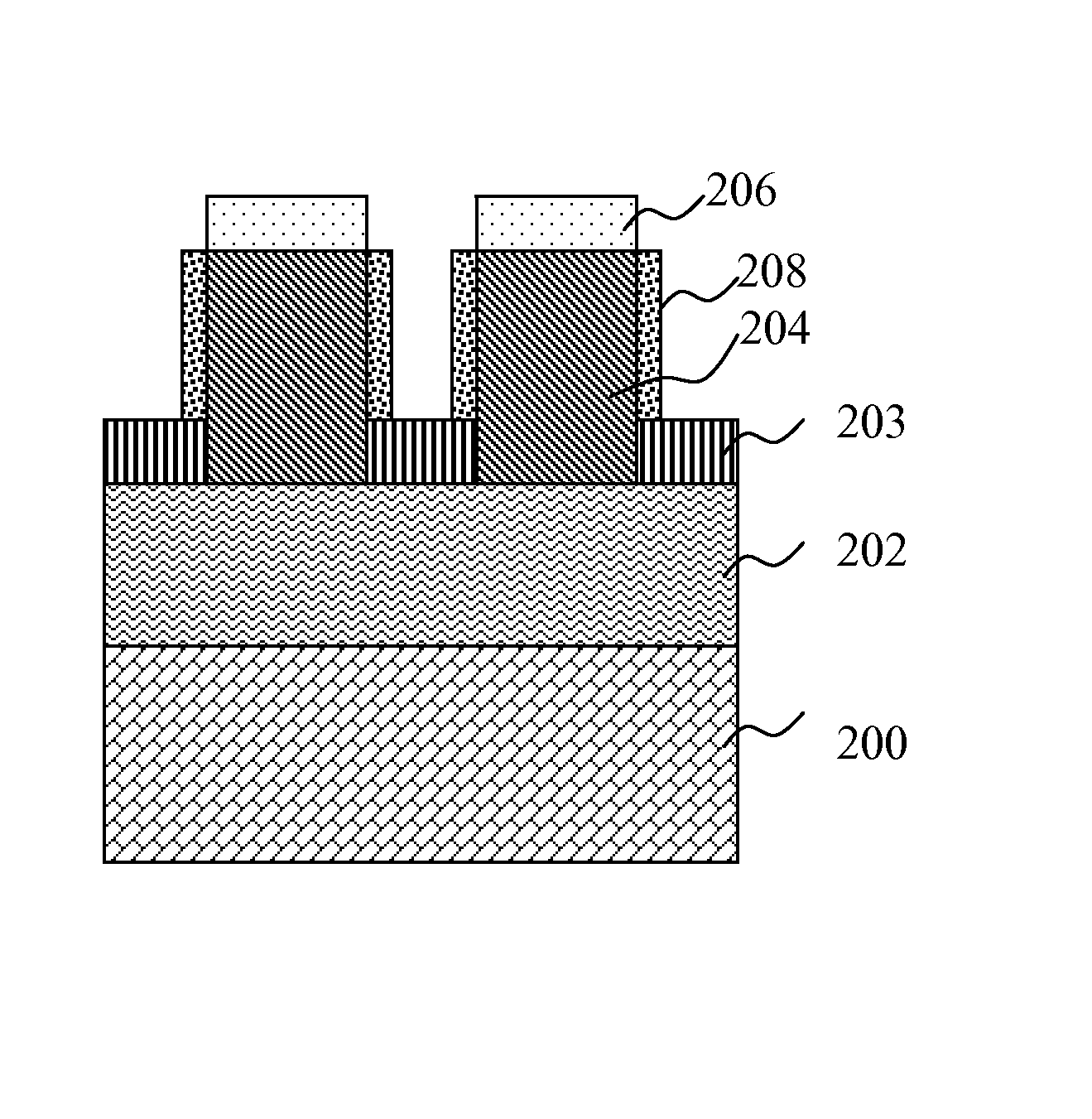
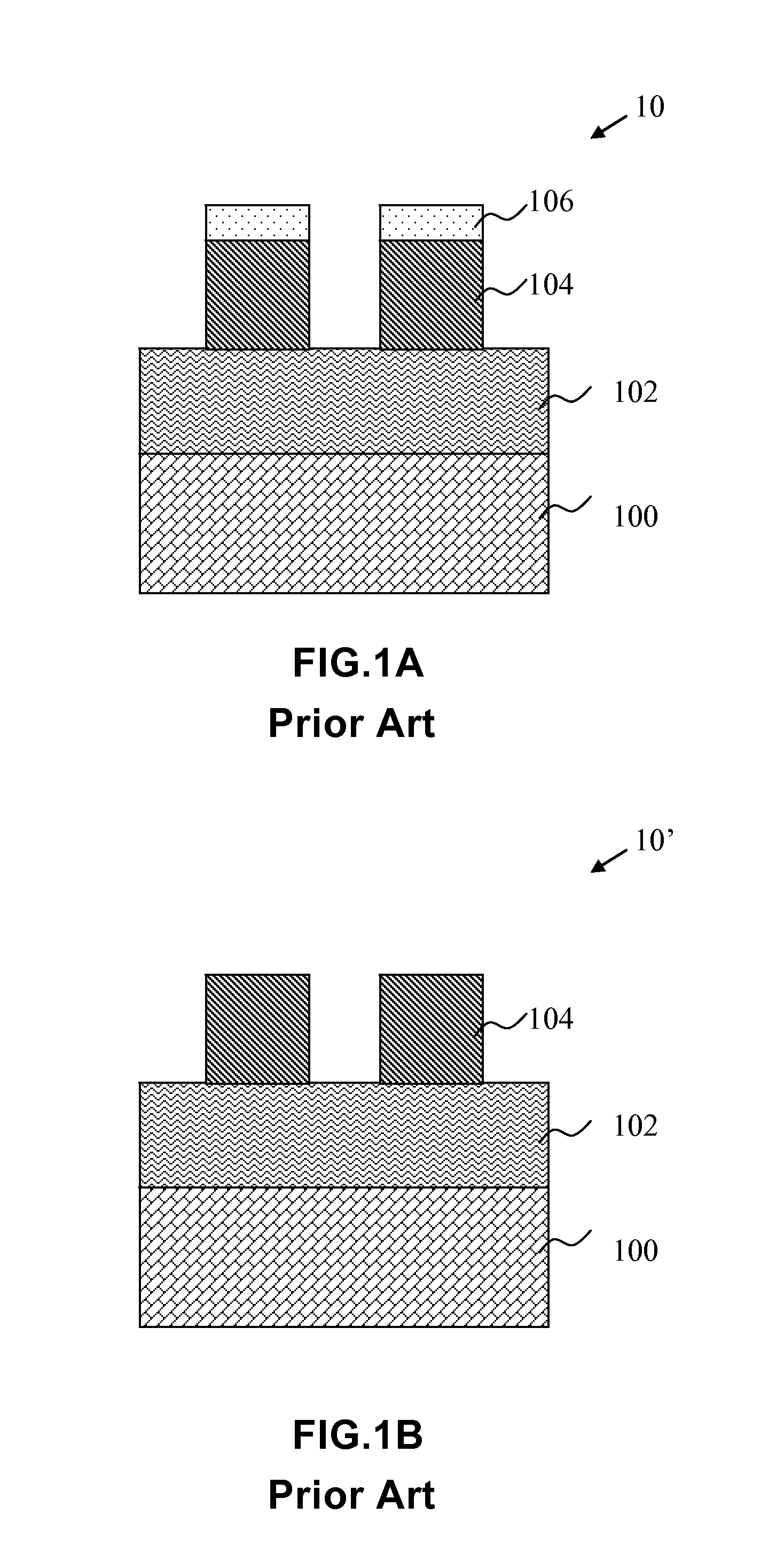
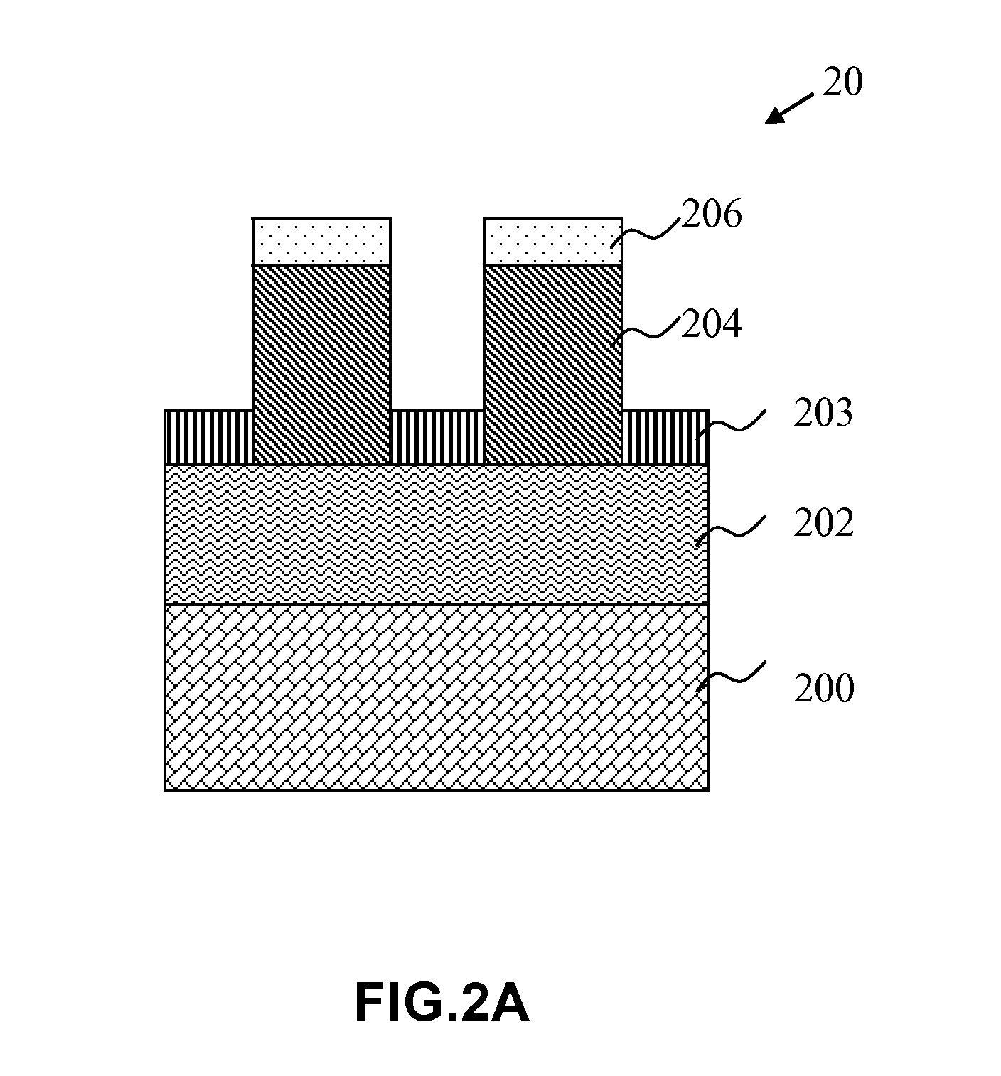
Embodiment Construction

[0054]The detailed description set forth below in connection with the appended drawings is intended as a description of some of the example embodiments, and is not intended to completely describe all possible embodiments. That is, there is no intention to be bound by any expressed or implied theory presented in the preceding technical field, background, or the following detailed description of example embodiments. It is to be understood that the same or equivalent functions may be accomplished by different embodiments.

[0055]The terms “first”, “second”, and the like in the description and the claims, if any, may be used for distinguishing between similar elements and not necessarily for describing a particular sequential or chronological order. It is to be understood that the terms so used are interchangeable under appropriate circumstances such that the embodiments described herein are, for example, capable of use in sequences other than those illustrated or otherwise described here...


PUM


Abstract

A semiconductor device and manufacturing method for the same are disclosed. The method includes providing a substrate that has an insulator layer and a semiconductor layer overlying the insulator layer. The method further includes forming a hard mask layer pattern on the semiconductor layer and etching the semiconductor layer using the patterned hard mask layer to form portions having different thickness in the semiconductor layer. The method also includes performing an oxygen-based treatment on the semiconductor layer to form a supporting oxide layer. A portion of the semiconductor layer is buried in the supporting oxide layer.

Description

CROSS-REFERENCES TO RELATED APPLICATIONS[0001]This application claims priority to Chinese Patent Application No. 201110266369.3, filed on Sep. 9, 2011 and entitled “Semiconductor Device and manufacturing method for the same”, which is incorporated herein in its entirety by reference.BACKGROUND OF THE INVENTION[0002]1. Field of the Invention[0003]This disclosure relates to semiconductor technology, and more particularly, to a semiconductor device and manufacturing method for the same.[0004]2. Description of the Related Art[0005]As semiconductor processing technology advances, the critical dimension (CD) of a semiconductor device continuously scales down. In such case, requirements for semiconductor manufacturing processes have become more stringent.[0006]Taking a fin field effect transistor (FinFET) as an example, as the CD of the semiconductor device scales down, it is almost impossible to form a desired dimension of the fin, e.g., a width of the fin, by patterning with lithography....

Claims


Application Information

Patent Timeline
Patent Type & Authority Patents(United States)
IPC IPC(8): H01L21/00
CPCH01L21/02252H01L29/66795H01L21/02238H01L29/785
Inventor HONG, ZHONGSHAN
Owner SEMICONDUCTOR MANUFACTURING INTERNATIONAL (BEIJING) CORP
Why Eureka
Try Eureka