Organic luminescent device including a first electrode, two or more organic layers and a second electrode and a production method for the same

a luminescent device and organic compound technology, applied in the direction of luminescent compositions, organic semiconductor devices, thermoelectric devices, etc., can solve the problems of inability to select a material for the hole injection layer, the device performance is affected by an electric field applied to the device, and the interface between the electrode formed of metal, metal oxides or conductive polymers and the organic compound layer is unstable, etc., to achieve excellent device performance, such as efficiency, luminance, or driving voltage

Active Publication Date: 2014-04-01
LG DISPLAY CO LTD
View PDF29 Cites 1 Cited by
  • Summary
  • Abstract
  • Description
  • Claims
  • Application Information

AI Technical Summary

Benefits of technology

[0020]The organic light emitting device according to the present invention has a low energy barrier for charge injection and an excellent charge transport ability of a charge transport organic compound layer so as to have excellent device performances, such as efficiency, luminance, or a driving voltage. Further, since various materials can be used as a material for an electrode, a device manufacturing process can be simplified. In addition, since the anode and the cathode can be formed of the same material, a stacked organic light emitting device having a high luminance can be obtained. Since an electrode made of ITO, IZO and the like having a high Fermi energy level can be used as a cathode and an intermediate electrode, an organic light emitting device having a high luminance can be manufactured. Further, since the transparent ITO and IZO electrodes can be used as both an anode and a cathode, a transparent organic light emitting device can be manufactured.

Problems solved by technology

However, an interface between the electrode formed of metal, metal oxides, or conductive polymers and the organic compound layer is unstable.
Accordingly, heat applied from the outside, internally generated heat, or an electric field applied to the device has an adverse effect on performance of the device.
However, since the hole injection layer needs to be selected in view of an HOMO energy level of a hole transport layer or a light emitting layer close to the hole injection layer as well as in view of the Fermi energy level of the anode, there is a limitation to select a material for the hole injection layer.
However, most of the above materials are unstable.
Due to the limitation in the selection of electron materials, most of organic light emitting devices have a structure in which light is emitted through a transparent anode.
The semi-transparent cathode materials have a problem in that their conductivity decreases because electrodes have to be formed with thin films in order to improve their transparency.

Method used


Image

  • Organic luminescent device including a first electrode, two or more organic layers and a second electrode and a production method for the same
  • Organic luminescent device including a first electrode, two or more organic layers and a second electrode and a production method for the same
  • Organic luminescent device including a first electrode, two or more organic layers and a second electrode and a production method for the same

Examples


example

Example 1

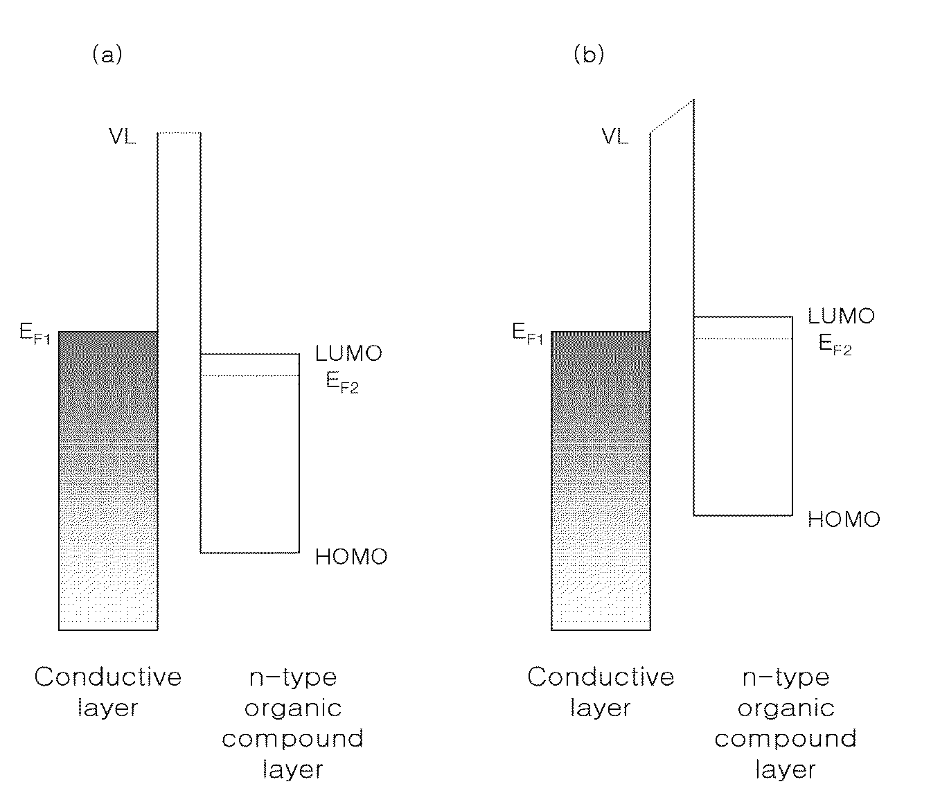
[0157]Measurement of HOMO and LUMO Energy Levels of HAT Using UPS and UV-VIS Absorption Methods

[0158]Hexanitrile hexaazatriphenylene (HAT) was used as the organic material having n-type semiconductor characteristics. In order to measure the HOMO level of HAT, a UPS (Ultraviolet photoelectron spectroscopy) method was used. In the method, kinetic energy of electrons that are discharged from a sample when vacuum UV rays (21.20 eV) emitted from the He lamp are radiated onto the sample in a ultravacuum (−8 torr) is analyzed to detect a work function of metal, or to detect ionization energy of organic material, that is, the HOMO level and the Fermi energy level. That is, the kinetic energy of electrons that are discharged from the sample when the vacuum UV rays (21.20 eV) are radiated onto the sample is a difference between 21.2 eV that is vacuum UV energy and electron binding energy of the sample to be measured. Accordingly, a binding energy distribution of molecules in the mate...

example 2

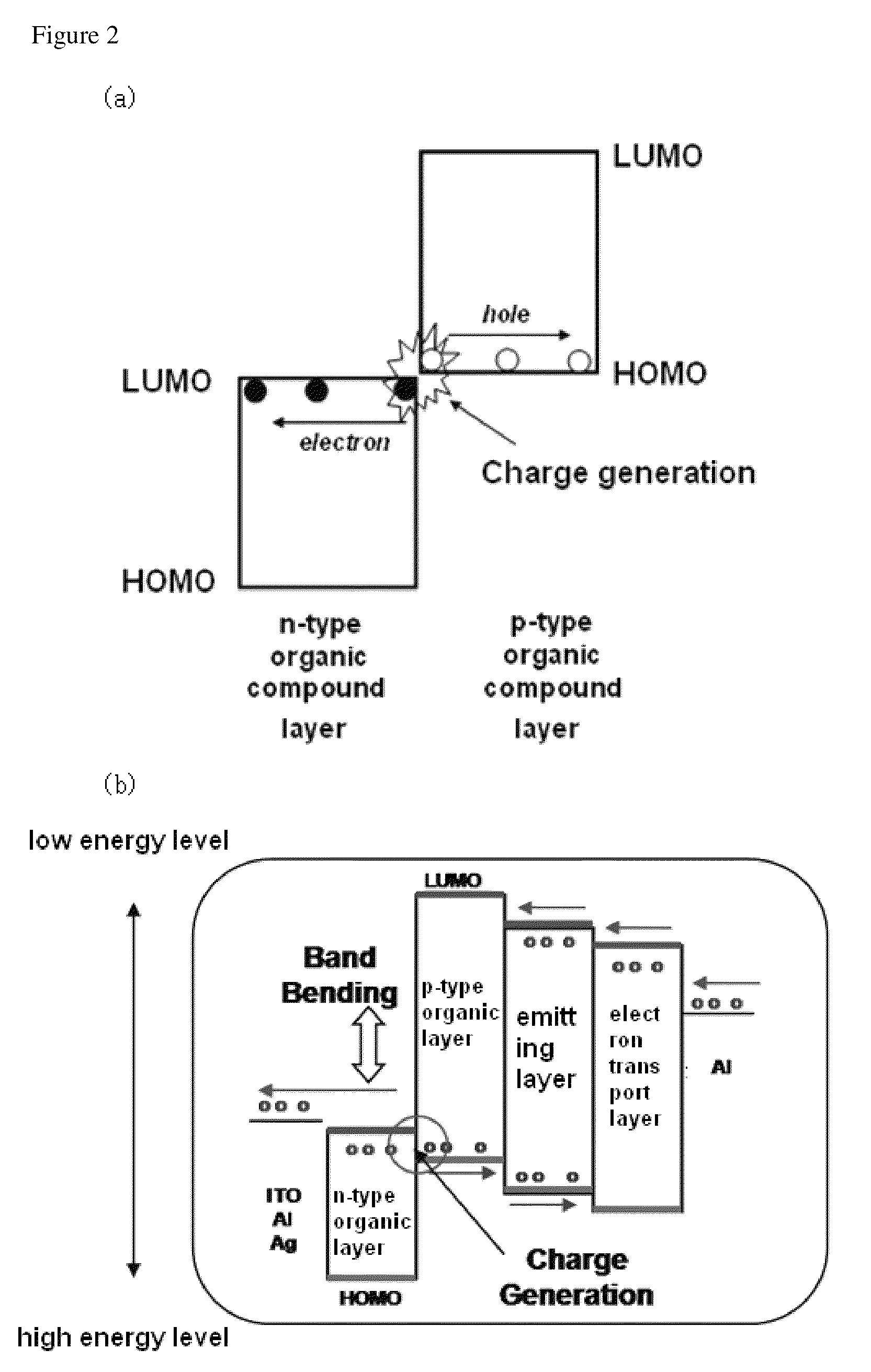
[0162]On a glass substrate, an IZO (indium zinc oxide) conductive layer of a thickness of 1000 Å was formed using a sputtering apparatus, then HAT of Formula 2-1 was vacuum deposited on the IZO layer by heating to a thickness of about 500 Å to form a transparent anode having the IZO conductive layer and the n-type organic layer. The HOMO energy level of HAT was about 9.78 eV. Subsequently, NPB of Formula 2-2 was vacuum deposited by heating thereby forming a p-type hole transport layer having a thickness of about 400 Å. Alq3 (HOMO level=about 5.7 eV) of Formula 2-3 was vacuum deposited on the p-type hole transport layer by heating while doping 6 volume % of the C545T dopant of Formula 2-4 to a thickness of about 300 Å to form a light emitting layer.

[0163]30 volume % Mg was doped into the compound of Formula 2-5, and vacuum deposited by heating to a thickness of 200 Å to form the electron transport layer on the emitting layer. Aluminum layers having a thickness of 1000 Å were sequenti...

example 3

[0165]An organic light emitting device was manufactured by using the same method as Example 2, except that the electron transport layer was doped with 10 volume % of Ca instead of Mg.


PUM


Abstract

Disclosed is an organic light emitting device comprising a first electrode, two or more organic compound layers, and a second electrode, wherein the first electrode comprises a conductive layer and an n-type organic compound layer which is in contact with the conductive layer, one of the organic compound layers interposed between the n-type organic compound layer of the first electrode and the second electrode is a p-type organic compound layer forming an NP junction together with the n-type organic compound layer of the first electrode, energy levels of the layers satisfy the following Expressions (1) and (2), and one or more layers interposed between the p-type organic compound layer and the second electrode are n-doped with alkali earth metal:0 eV<EnL−EF1≦4 eV  (1)EpH−EnL≦1 eV  (2)where EF1 is a Fermi energy level of the conductive layer of the first electrode, EnL is an LUMO (lowest unoccupied molecular orbital) energy level of the n-type organic compound layer of the first electrode, and EpH is an HOMO (highest occupied molecular orbital) energy level of the p-type organic compound layer forming the NP junction together with the n-type organic compound layer of the first electrode.

Description

[0001]This application is a 35 U.S.C. §371 National Stage entry of International Application No. PCT / KR2009 / 000283, filed on Jan. 19, 2009, and claims priority to Korean Application No. 10-2008-0005812, filed on Jan. 18, 2008, which are all hereby incorporated by reference in their entireties.TECHNICAL FIELD[0002]The present invention relates to an organic light emitting device that has a low energy barrier for charge injection from an electrode to an organic compound layer, a low driving voltage, and high efficiency and luminance, and to a method for manufacturing the organic light emitting device.BACKGROUND ART[0003]In general, an organic light emitting device includes two electrodes and an organic compound layer interposed between the electrodes. In the organic light emitting device, electrons and holes are injected into the organic compound layer from the two electrodes, and a current is converted into visible light. In the organic light emitting device, in order to improve perf...

Claims


Application Information

Patent Timeline
Patent Type & Authority Patents(United States)
IPC IPC(8): H01L29/08
CPCH01L51/5092H01L2251/552C09K2211/1037H01L51/5004H01L51/5052C09K2211/1033H01L51/5084H10K50/11H10K2101/40H10K50/167H10K50/171H10K2101/30H10K50/165H05B33/14H05B33/18C09K11/06H10K50/00
Inventor KANG, MIN-SOOSON, SE-HWANNOH, JEOUNG-KWEN
Owner LG DISPLAY CO LTD
Why Eureka
Try Eureka