Resonant power factor correction converter

a power factor and converter technology, applied in the direction of electric variable regulation, process and machine control, instruments, etc., can solve the problems of transformer design difficulties, high current stress, and increase the loss of mosfet, so as to reduce the burden of low-voltage-drop semiconductor switches and high current stress

Active Publication Date: 2014-04-08
MYPAQ HLDG LTD
View PDF176 Cites 19 Cited by
  • Summary
  • Abstract
  • Description
  • Claims
  • Application Information

AI Technical Summary

Benefits of technology

[0019]A power converter is configured to operate over a relatively large input voltage range and to provide either a single somewhat regulated isolated DC output, or multiple highly-regulated isolated low-voltage DC outputs and a high power factor input with a low overall cost and a high efficiency. In some embodiments, an isolation transformer turns-ratio is on the order of 1, 2, or 4, allowing for flexibility in transformer construction to match a given bobbin, as well as simplifying low-EMI transformer design. Furthermore, control used to obtain high power factor input current waveforms with low total-harmonic-distortion is relatively simple.
[0020]The power converter includes an isolated resonant converter at the input to produce a high-efficiency isolated converter without switching losses, without the EMI issues associated with hard-switching, and without the need for expensive diodes to mitigate diode reverse recovery losses. Switches within the resonant converter are driven at approximately 50% duty cycle with dead-time delay. Control of the converter to achieve high power factor is simplified since the input current automatically tracks the input voltage minus the reflected output voltage.
[0022]In some applications, the single output bus is adequate, thus providing a highly efficient, inexpensive, single-stage isolated converter with power factor correction. In most applications, however, post-processing converters are used to convert the single voltage output bus to the appropriate output voltages. In most cases, the post-processing converters are buck-type converters. Since the resonant converter has only a single output, and each post-processing converter is separately controlled, there are no cross-regulation issues. Furthermore, the design can easily be modified to accommodate any desired output voltages. This is unlike conventional converters that produce multiple outputs from multiple transformer windings. In such a conventional design, difficulties arise in designing the transformer due to the consideration of the exact ratio of each output voltage and the effect of rectifier and inductive voltage drops.
[0023]If the output post-processing converters are buck-type converters, they can easily be configured to produce soft-switching through resonant or quasi-resonant configurations. Soft-switching can also be easily accomplished by operating the buck-type converters in critical or discontinuous conduction mode, if the low voltage output bus from the resonant converter is more than double the voltage of any of the outputs. For example, if the output from the resonant converter is 20V to 24V (allowing for 4V of low-frequency line ripple), then outputs of 5V and 3.3V can be derived from soft-switched buck-type converters operating in critical or discontinuous conduction mode. An output voltage of 12V is achieved with minimal switching loss since the voltage at the switching point of the semiconductor switches in the resonant converter is 2Vout-Vin, where Vin is the low voltage output bus from the resonant converter. The voltage at the switching points varies from 0V to 8V if the input varies from 20V to 24V. In this example, where the semiconductor switches are MOSFETs, the use of a single 24V output from the resonant converter has the additional benefit that MOSFETs are most efficient when used at low voltages, and power converter MOSFETs are typically optimized for cost and performance at the 30V level, a voltage level that provides a reasonable design margin around a 24V bus.
[0024]The resonant converter of the present invention is configured to operate with soft-switching of the semiconductor switches, thus overcoming the EMI issues associated with hard-switched converters. Conventional boost-type power factor correction circuits often require an expensive high-voltage Schottky diode, such as a Silicon Carbide diode, to mitigate reverse recovery losses. The resonant converter of the present invention overcomes this problem in two ways. First, the output diodes of the resonant converter are switched at zero current, so there is no reverse recovery. Second, the output diodes are low voltage diodes, so inexpensive low-voltage Schottky diodes are used in the resonant converter rather than the high-voltage Schottky diode used by conventional boost power factor correction converters.
[0026]Conventional converters that utilize resonant converters for an output stage put a high current stress on the output rectifier. If synchronous MOSFETs are used for the rectification stage (a configuration used for high-efficiency, low voltage output), then the MOSFET losses are increased by a factor of 2 or more by the conventional resonant converter waveform. The power converter of the present invention overcomes this problem by using a higher voltage at the output of the resonant converter, enabling the possibility of using Schottky or fast-recovery diodes rather MOSFETs at the output of the transformer. Diodes dissipate power primarily as a function of their average current, rather than root mean square (rms) current, so the use of a resonant topology does not substantially change the losses incurred by diodes. In the power converter of the present invention, the burden of low-voltage-drop semiconductor switches is shifted to the post-regulating buck-type converters, where the root mean square current in the MOSFETs can be kept low.

Problems solved by technology

In such a conventional design, difficulties arise in designing the transformer due to the consideration of the exact ratio of each output voltage and the effect of rectifier and inductive voltage drops.

Method used


Image

  • Resonant power factor correction converter
  • Resonant power factor correction converter
  • Resonant power factor correction converter

Examples


first embodiment

[0045]FIG. 4 illustrates an exemplary schematic diagram of the power train components of the power converter 100 of FIG. 3. The power converter 100 shown in FIG. 4 is configured to include an LLC resonant half-bridge converter followed by buck-type converters. The power source 110 generates the input AC power supply voltage VACin. A capacitor C1, a capacitor C2, a transformer TX3, and an inductor L2 form a line filter for filtering out EMI. The inductor L2 acts as a differential mode filter to filter out the resonant-frequency current. Diodes D1, D2, D3, and D4 form a full-wave bridge rectifier configured to rectify the input line voltage. A capacitor C3, a capacitor C4, a capacitor C5, an inductor L1, a transistor Q1, a transistor Q2, and an isolation transformer TX1 form a resonant half-bridge converter. The transistors Q1 and Q2 function as switches. The capacitor C3 and the capacitor C4 form both the half-bridge center tap as well as input line filtering. In some embodiments, a ...

second embodiment

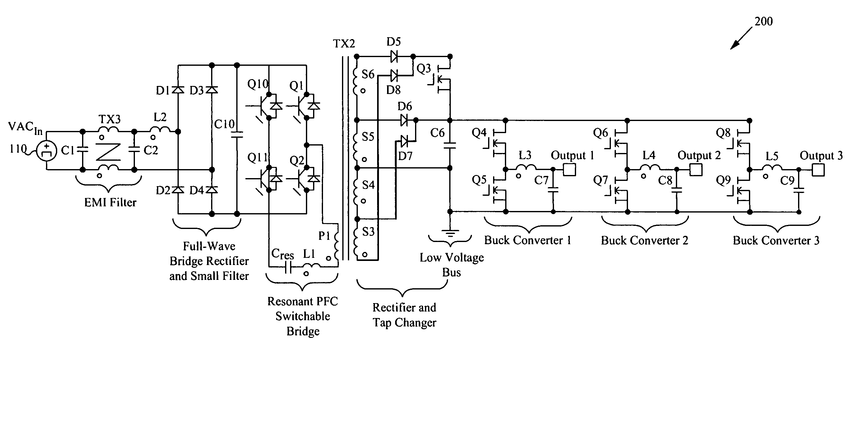
[0052]FIG. 5 illustrates an exemplary schematic diagram of the power train components of the power converter of FIG. 3. The power converter 100′ of FIG. 5 is similar to the power converter 100 shown in FIG. 4, except that the transformer TX1 is replaced by the transformer TX2. The transformer TX2 includes four transformer secondaries instead of two transformer secondaries as in the transformer TX1. Each of the four transformer secondaries of the transformer TX2 is coupled to a rectifier, specifically the diodes D5, D6, D7, D8. The diodes D5, D6, D7, D8 provide rectification of the resonant current output from the transformer TX2.

[0053]The power converter 100′ also differs from the power converter 100 in that the power converter 100′ includes a transistor Q3 coupled to each of the additional two transformer secondaries. In some embodiments, the transistor Q3 is a MOSFET. In other embodiments, the transistor Q3 can be any other type of semiconductor switching device. The transistor Q3...

third embodiment

[0056]FIG. 6 illustrates an exemplary schematic diagram of the power train components of the power converter of FIG. 3, including a switchable bridge. The power converter 200 of FIG. 6 is similar to the power converter 100′ shown in FIG. 5, except that the half-bridge converter is replaced by a switchable bridge converter. Specifically, the capacitors C3 and C4 of the power converter 100′ are replaced by transistors Q10 and Q11, respectively, in the power converter 200. The transistors Q1, Q2, Q10, Q11, the capacitor C5, the inductor L1, and the isolation transformer TX2 form a resonant PFC switchable bridge converter. The function of the two capacitors C3 and C4 (FIG. 5) is incorporated into the resonant capacitor Cres of FIG. 6. The DC bias voltage that is blocked by the capacitors C3 and C4 (FIG. 5) is added to the AC voltage across resonant capacitor Cres. Further, an additional capacitor C10 is coupled across the output of the full-wave bridge rectifier to function as a filter,...


PUM


Abstract

An AC-to-DC power converter configured to provide power factor correction and a single isolated low-voltage output. The power converter includes a single-stage resonant power converter including an isolation transformer, a resonant tank, a rectifier, and a bulk storage capacitor coupled to an output of the isolation transformer. In typical applications, at least one non-isolated power converter is coupled to the output of the single-stage isolated power factor correction converter.

Description

FIELD OF THE INVENTION[0001]The invention relates to power converters. More particularly, the invention relates to a resonant power factor correction converter.BACKGROUND OF THE INVENTION[0002]A power supply is a device or system that supplies electrical or other types of energy to an output load or group of loads. The term power supply can refer to a main power distribution system and other primary or secondary sources of energy. Power conversion refers to the conversion of one form of electrical power to another desired form and voltage, for example converting 115 or 230 volt alternating current (AC) supplied by a utility company to a regulated lower voltage direct current (DC) for electronic devices, referred to as AC-to-DC power conversion.[0003]A switched-mode power supply, switching-mode power supply or SMPS, is a power supply that incorporates a switching regulator. While a linear regulator uses a transistor biased in its active region to specify an output voltage, an SMPS ac...

Claims


Application Information

Patent Timeline
Patent Type & Authority Patents(United States)
IPC IPC(8): H02M3/335
CPCH02M2001/007Y02B70/126H02M1/4241Y02B70/10H02M1/007
Inventor JUNGREIS, AARONGARRITY, PAUL
Owner MYPAQ HLDG LTD
Why Eureka
Try Eureka