Methods and apparatus to review defects using scanning electron microscope with multiple electron beam configurations

a scanning electron microscope and electron beam technology, applied in the direction of material analysis using wave/particle radiation, instruments, nuclear engineering, etc., can solve the problem of almost always detected defects

Active Publication Date: 2014-05-06
KLA TENCOR TECH CORP
View PDF13 Cites 249 Cited by
  • Summary
  • Abstract
  • Description
  • Claims
  • Application Information

AI Technical Summary

Problems solved by technology

However, there are almost always some defects that are detected by the inspection system but do not show up (i.e. are not visible to) the review system.

Method used


Image

  • Methods and apparatus to review defects using scanning electron microscope with multiple electron beam configurations
  • Methods and apparatus to review defects using scanning electron microscope with multiple electron beam configurations
  • Methods and apparatus to review defects using scanning electron microscope with multiple electron beam configurations

Examples


Embodiment Construction

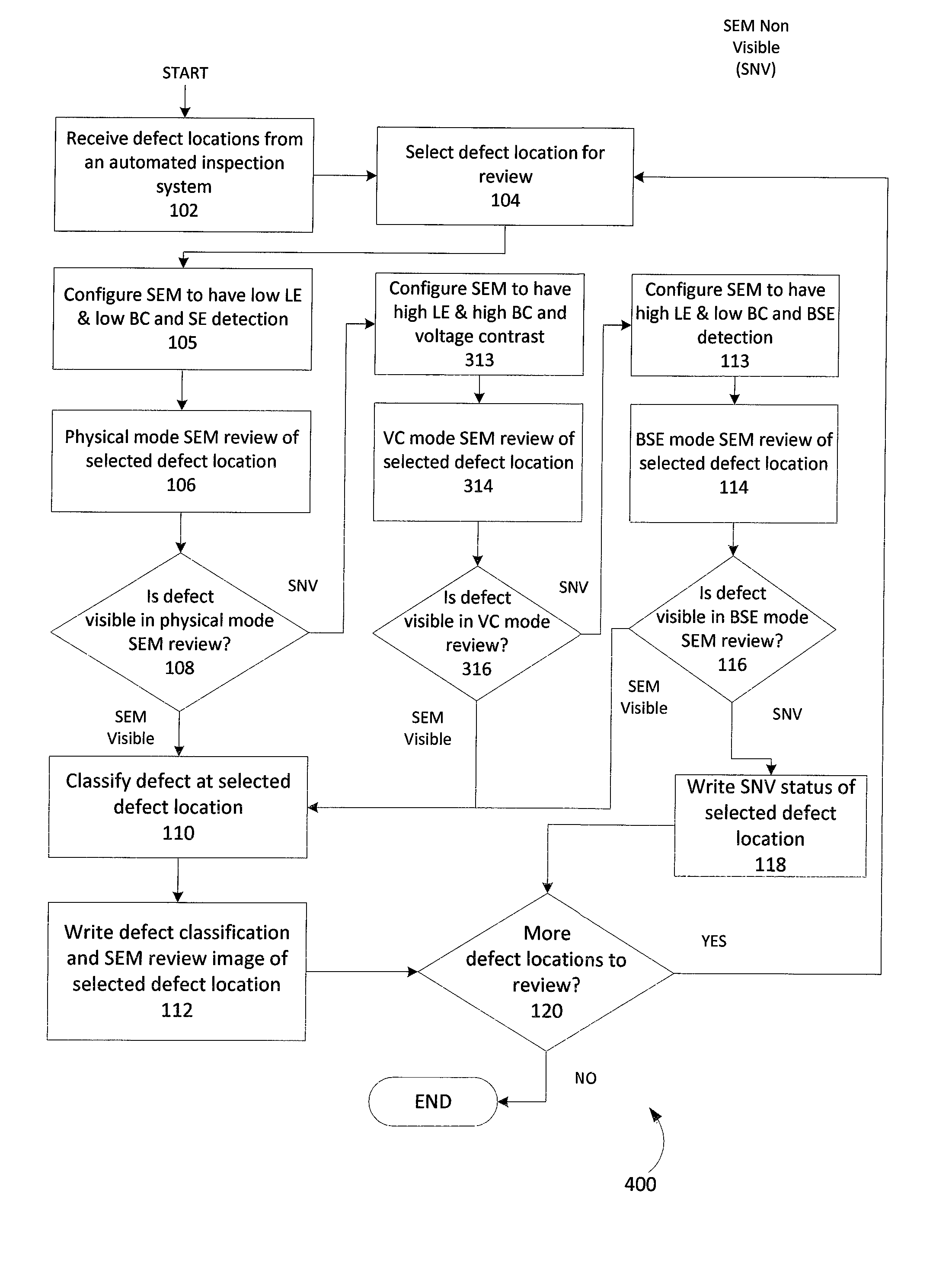
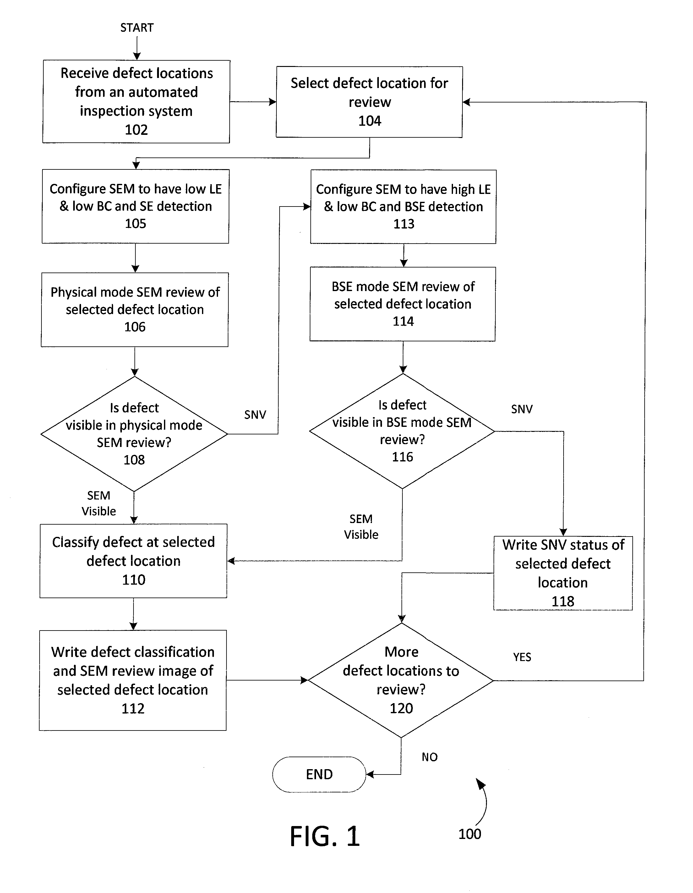
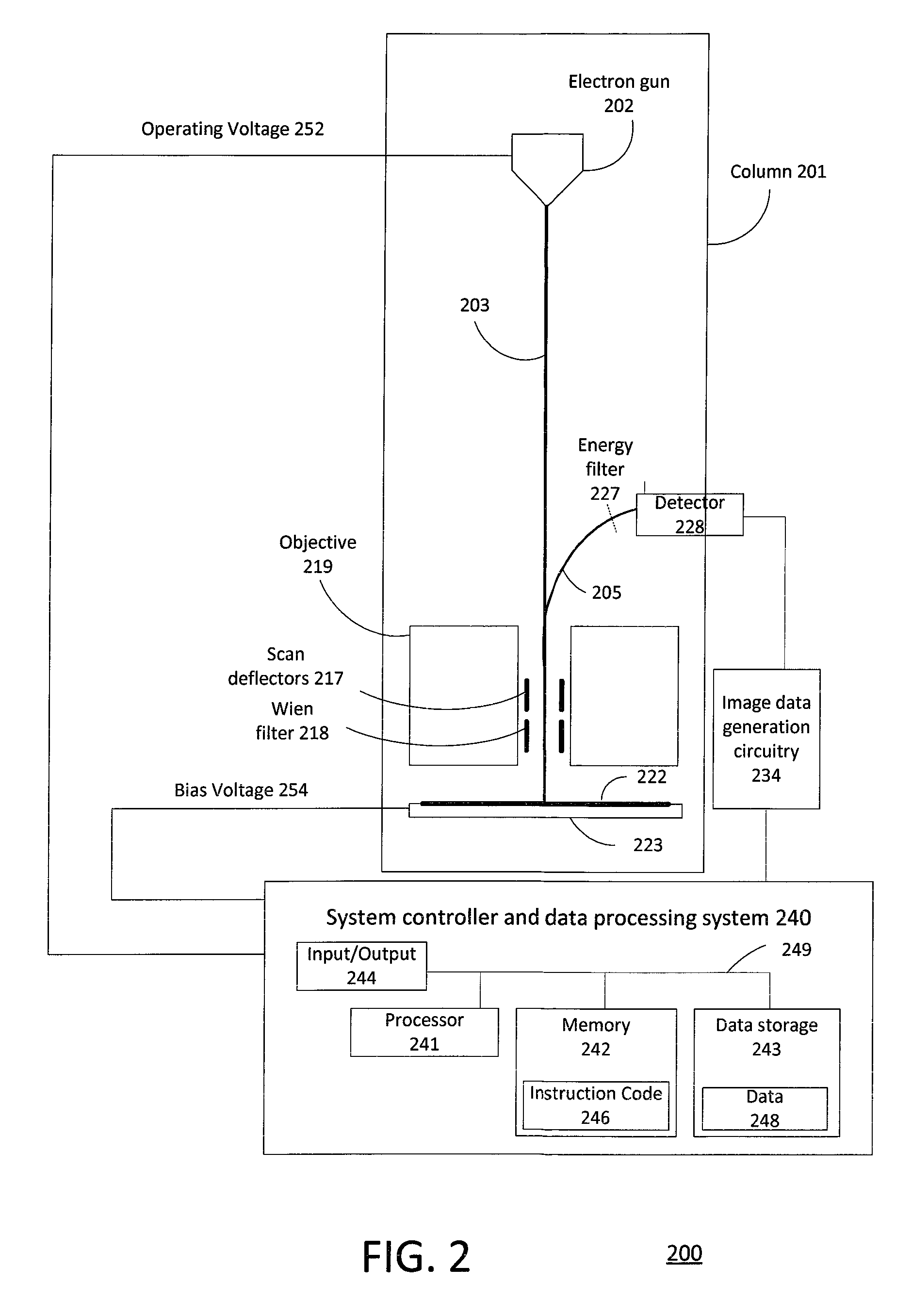
[0013]FIG. 1 is a flow chart of a method 100 of automated defect review using an automated review system with SEM imaging in accordance with an embodiment of the invention. In one embodiment, the automated review apparatus may be an apparatus 200 such as that depicted in FIG. 2.

[0014]Per step 102, the apparatus may receive defect locations from an automated inspection apparatus. The inspection apparatus may determine the defect locations using bright or dark field optical imaging or by electron beam imaging. Multiple defect locations may be received for review.

[0015]Per step 104, the apparatus may select a defect location for review from the multiple defect locations. In addition, the SEM may be configured to have a low landing energy (LE) and low beam current (BC) and to detect secondary electrons (SE) per step 105. This configuration may be referred to as a physical mode. The low landing energy beam may be suitable to obtain image data from a layer at or near the surface of the ta...


PUM


Abstract

One embodiment relates to a method of reviewing defects using a scanning electron microscope (SEM). A defect location having a defect for review is selected, and the SEM is configured to be in a first imaging configuration. The selected defect location is imaged using the SEM to generate a first SEM image of the selected defect location. A determination is made as to whether the defect is visible or non-visible in the first SEM image. If the defect is non-visible in the first SEM image, then the SEM is configured to be into a second imaging configuration, the selected defect location is imaged using the SEM to generate a second SEM image of the selected defect location, and a further determination is made as to whether the defect is visible or non-visible in the second SEM image. Other embodiments, aspects and features are also disclosed.

Description

BACKGROUND OF THE INVENTION[0001]1. Field of the Invention[0002]The present invention relates to methods and apparatus for inspection and review of semiconductor wafers and other manufactured substrates.[0003]2. Description of the Background Art[0004]An automated defect review system generally receives a defect location that is determined previously by an automated inspection system. The inspection system may determine the defect location using bright or dark field optical imaging or by electron beam imaging.[0005]The defect review system may then use a scanning electron microscope (SEM) having a pre-set electron beam configuration, usually in a secondary electron mode, to obtain an image at the defect location. However, there are almost always some defects that are detected by the inspection system but do not show up (i.e. are not visible to) the review system. These defects are conventionally classified as SEM non-visible (SNV) defects.SUMMARY[0006]One embodiment relates to a meth...

Claims


Application Information

Patent Timeline
Patent Type & Authority Patents(United States)
IPC IPC(8): H01J37/28
CPCH01J37/222H01J37/28H01J2237/24592
Inventor MACDONALD, PAULXIAO, HONG
Owner KLA TENCOR TECH CORP
Why Eureka
Try Eureka