Electron beam apparatus

a charge-particle, electron-beam technology, applied in the field of charge-particle-beam apparatus, can solve the problems of electron optics producing large off-axis aberrations, mask or wafer damage during semiconductor fabrication process, and electron optics can produce large radiation damage to samples, so as to reduce total emission current, improve imaging resolution, and reduce the effect of electron emission current density without reducing angular intensity

Inactive Publication Date: 2011-06-14
ASML NETHERLANDS BV
View PDF67 Cites 25 Cited by
  • Summary
  • Abstract
  • Description
  • Claims
  • Application Information

AI Technical Summary

Benefits of technology

[0009]A system and method in accordance with the present invention improves imaging resolution which is illustrated in several embodiments. One embodiment discloses a field emission cathode with a large tip radius to reduce electron emission current density without reducing angular intensity. Another embodiment discloses applying a large accelerating voltage across ground potential between the cathode and anode to reduce total emission current without reducing angular intensity. Another embodiment positions the beam limit aperture before condenser lens to reduce Coulomb effect generated before beam limit aperture. And yet another embodiment utilizes condenser lens excitation current to optimize image resolution without altering probe current. One other embodiment applies a high positive tube bias to the ground potential and a high negative sample bias to the ground potential to reduce objective aberrations and Coulomb effect. A system and method in accordance with the present invention adopts and modifies the Swing Objective Retarding Immersion Lens (SORIL) / objective lens to ameliorate aberration at large field of view and under electric drifting.
[0010]A system and method in accordance with the present invention provides improved throughput during sample inspection, review or material identification by utilizing the fast scanning ability of SORIL and also provides a large voltage difference between sample and detectors. This design makes the secondary electrons impinging on the detector with large kinetic energy, which is better for getting higher detection gain. Thereafter higher signal to noise ratio is provided to benefit image quality.
[0011]A system and method in accordance with the present invention provides a solution of topography analysis by adopting and modifying a multi-channels detector. Signals from the different channels can generate a stereo image in combination, finally ensuring a topography analysis of the defects of interest. The system and method can largely reduce on-axis and off-axis aberrations in scanning imaging, and as a result the field of view with high resolution is increased.

Problems solved by technology

Defects can occur on the mask or wafer during the semiconductor fabrication process.
However, radiation damage to the sample is another subject to consider while utilizing high kinetic energy electron beam.
Electron optics produces large off-axis aberrations when the field of view becomes large.

Method used


Image

  • Electron beam apparatus
  • Electron beam apparatus
  • Electron beam apparatus

Examples


Embodiment Construction

[0021]Reference will now be made in detail to specific embodiments of the invention. Examples of these embodiments are illustrated in accompanying drawings. While the invention will be described in conjunction with these specific embodiments, it will be understood that it is not intended to limit the invention to these embodiments. On the contrary, it is intended to cover alternatives, modifications, and equivalents as may be included within the spirit and scope of the invention as defined by the appended claims. In the following description, numerous specific details are set forth in order to provide a through understanding of the present invention. The present invention may be practiced without some or all of these specific details. In other instances, well known process operations are not described in detail in order not to unnecessarily obscure the present invention.

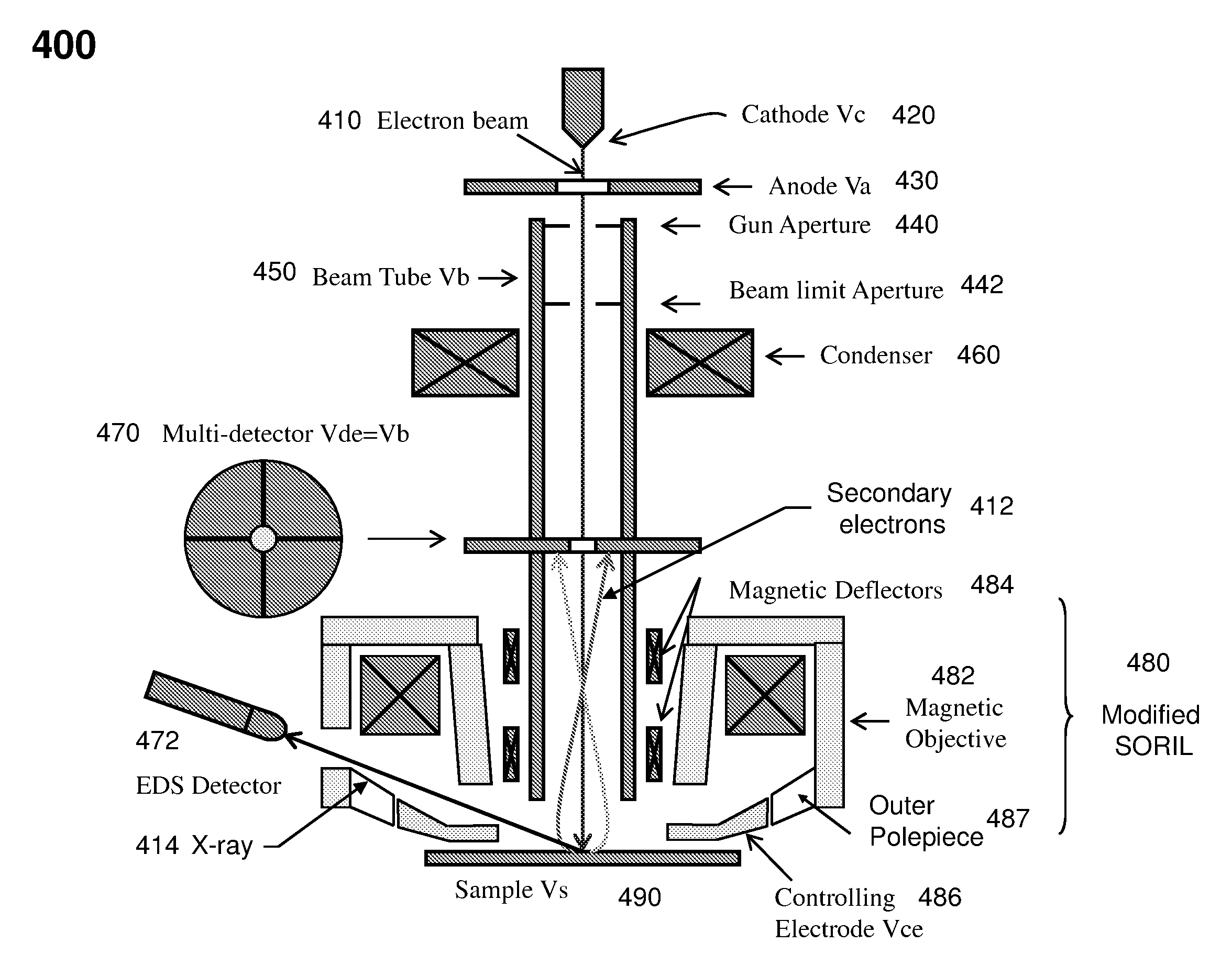
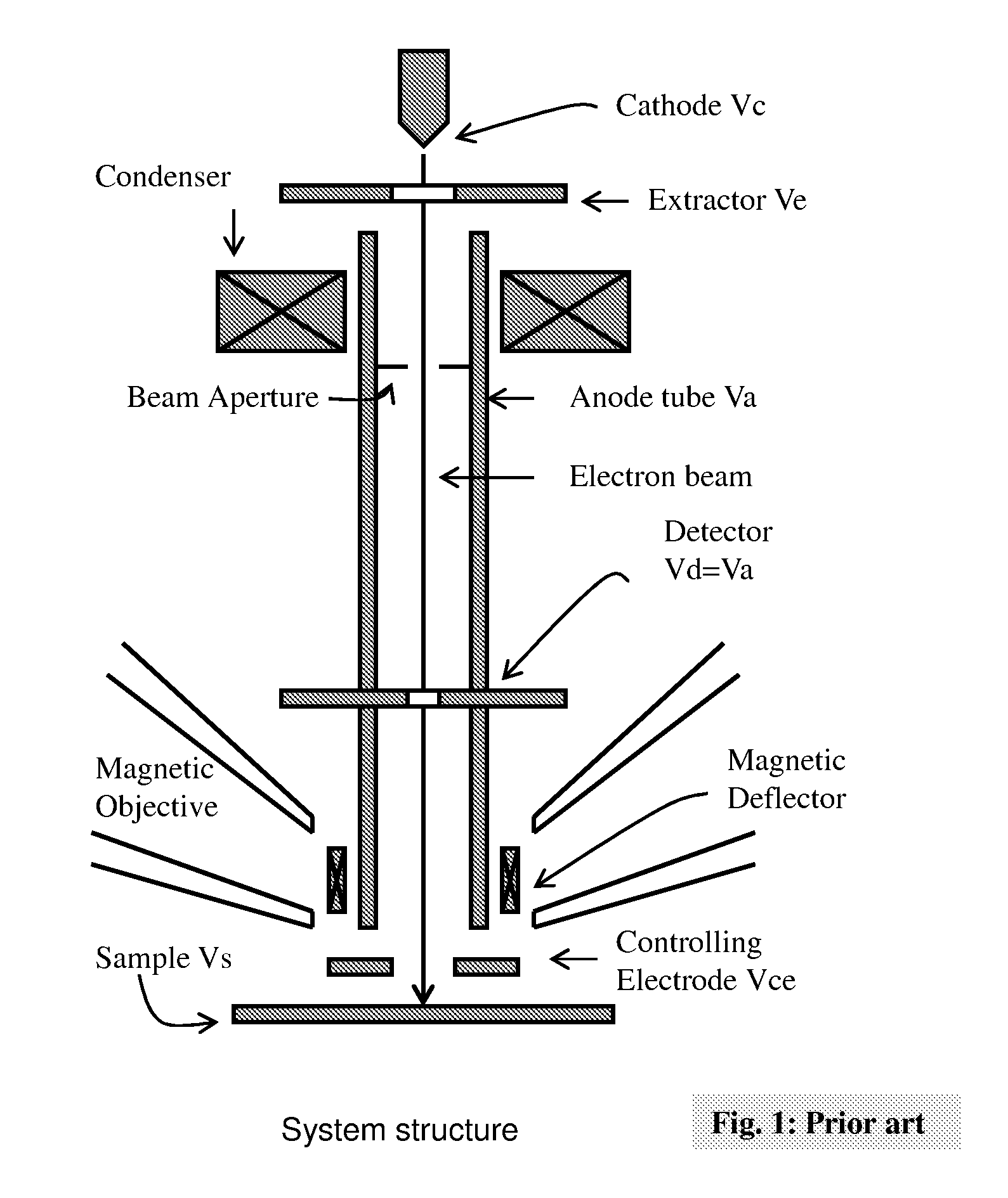
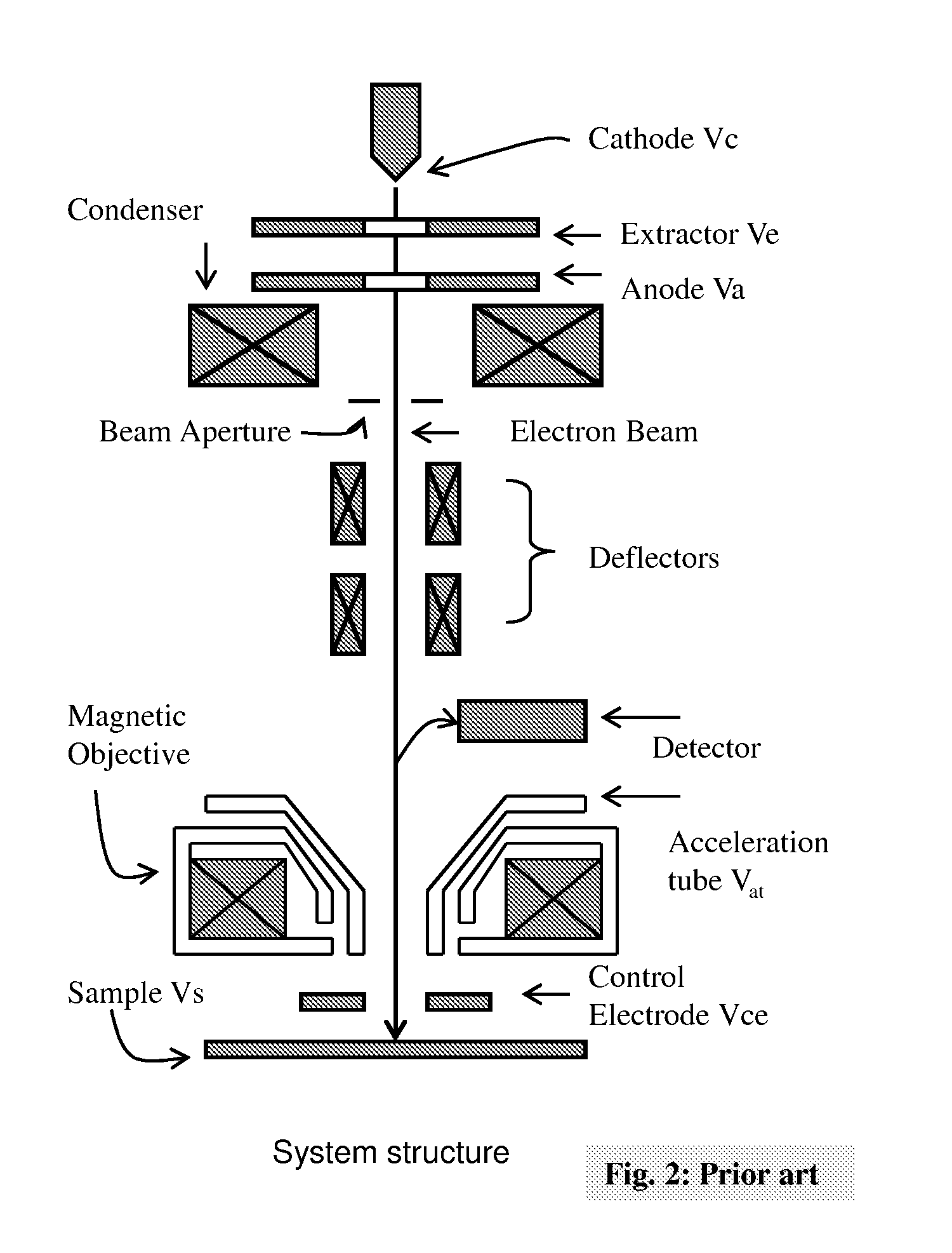
[0022]A charged particle beam apparatus which employs a scanning electron microscope for sample inspection and def...


PUM


Abstract

The present invention relates to a charged particle beam apparatus which employs a scanning electron microscope for sample inspection and defect review.The present invent provides solution of improving imaging resolution by utilizing a field emission cathode tip with a large tip radius, applying a large accelerating voltage across ground potential between the cathode and anode, positioning the beam limit aperture before condenser lens, utilizing condenser lens excitation current to optimize image resolution, applying a high tube bias to shorten electron travel time, adopting and modifying SORIL objective lens to ameliorate aberration at large field of view and under electric drifting and reduce the urgency of water cooling objective lens while operating material analysis.The present invent provides solution of improving throughput by utilizing fast scanning ability of SORIL and providing a large voltage difference between sample and detectors.

Description

RELATED APPLICATIONS[0001]Under 35 USC §120, this application is a Non-Provisional application and is related to co-pending U.S. patent application Ser. No. 12 / 130,879, filed on May 30, 2008, entitled “AN ELECTRON BEAM APPARATUS”; to U.S. patent application Ser. No. 11 / 668,846, filed on Jan. 30, 2007, entitled “CHARGE PARTICLE DETECTION DEVICES, all of which are incorporated herein by reference.FIELD OF THE INVENTION[0002]The present invention relates to a charged particle beam apparatus which employs a scanning electron microscope for sample inspection and defect review. However, it would be recognized that the invention has a much broader range of applicability.BACKGROUND OF THE INVENTION[0003]A charged particle beam apparatus typically employs a scanning electron microscopy (SEM), which is a known technique used in semiconductor manufacturing. Defects can occur on the mask or wafer during the semiconductor fabrication process. These defects impact yield to a great degree. Defect ...

Claims


Application Information

Patent Timeline
Patent Type & Authority Patents(United States)
IPC IPC(8): H01J49/44
CPCH01J37/073H01J37/244H01J37/28H01J2237/24592H01J2237/06341
Inventor CHEN, ZHONGWEIREN, WEIMINGWANG, JOELIU, XUEDONGDOU, JUYINGHE, FUMINCAO, FENGREN, YANGUO, XIAOLIHE, WEIXI, QINGPO
Owner ASML NETHERLANDS BV
Why Eureka
Try Eureka