Integrated measuring instrument

a technology of optical instruments and integrated parts, applied in the field of systems, can solve the problems of time-consuming and laborious wafer sectioning, less useful monitoring methods, and excessive slope of actual sidewalls, and achieve the effect of improving the efficiency or accuracy of microscopic measurements

Inactive Publication Date: 2006-01-17
FEI CO
View PDF39 Cites 27 Cited by
  • Summary
  • Abstract
  • Description
  • Claims
  • Application Information

AI Technical Summary

Benefits of technology

[0018]An object of the invention is to enhance the

Problems solved by technology

For example, although an ideal feature typically has vertical sidewalls, the actual sidewalls may have excessive slope that narrows or widens the feature below its top surface.
While useful in developing new processes, this method is less useful in monitoring production processes because the entire wafer is destroyed to measure a feature.
Moreover, it is time consuming to section the wafer at the correct position and view it in an SEM.
Because it displays a top view, CD SEM does not usually provide any information on the three-dimensional profile of such holes or conductors, and may not alert a process engineer if the sidewalls of a feature are deviated from the vertical.
Insulators and photoresist tend to become electrically charged by the electrons in the CD SEM, and this charging causes the edges of the feature image to blur, making measurements uncertain by between 2 nm and 25 nm.
A further drawback with electron microscopy is that the measurement needs to be performed in a high vacuum to prevent the probing electrons from being scattered by air molecules.
It takes considerable time to remove the air from an SEM sample chamber, thereby preventing rapid feedback and limiting the number of wafers that can be

Method used


Image

  • Integrated measuring instrument
  • Integrated measuring instrument
  • Integrated measuring instrument

Examples


Embodiment Construction

[0032]The term scatterometer is used herein as a general term to describe any instrument that directs light to a sample and determines characteristics of the sample by measuring light reflected or scattered from the sample. The term includes ellipsometer-based scatterometry, reflectometry, and similar techniques.

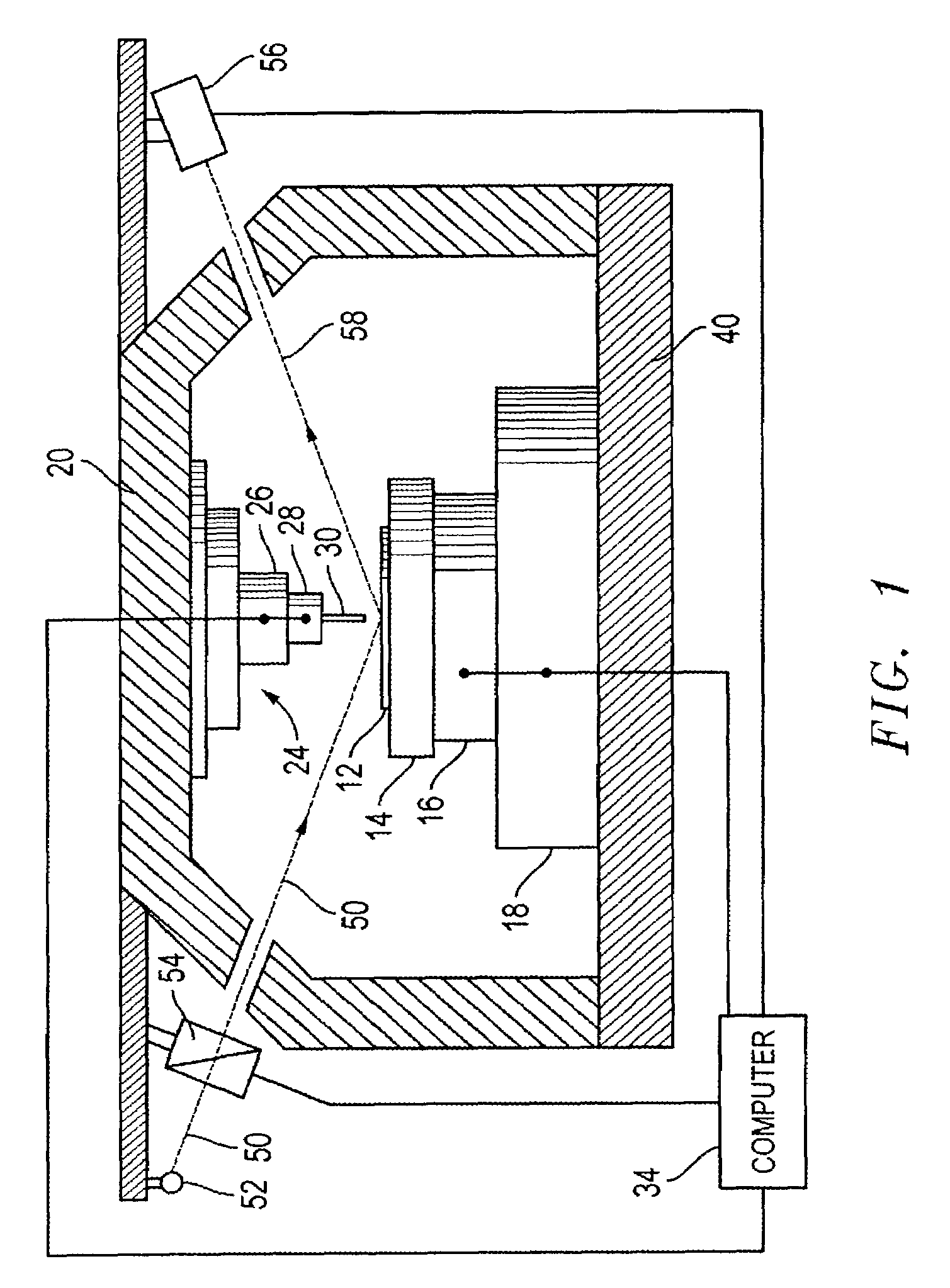
[0033]The invention combined an integrating optical instrument and an individual-feature-measuring instrument. One embodiment of the invention integrates in a single measurement instrument a scanning probe microscope, such as an AFM and an ellipsometer-based scatterometer. A wafer or other substrate supported on a single stage shared by both instruments can be probed by either the AFM or the scatterometer, either without repositioning the stage or by repositioning the stage by a predetermined offset. Thus, in a preferred embodiment, it is unnecessary to pick up the work piece and move it from one machine to another, thereby eliminating the time-consuming activity of locating...


PUM


Abstract

A surface analyzing system including in one system both an integrating optical instrument, such as a scatterometer, and individual-feature-measuring instrument, such as a scanning probe microscope or a beam imaging system, for example, a scanning electron microscope. In a preferred embodiment, the two instruments are capable of characterizing a wafer held on a common stage. The stage may be movable a predetermined displacement to allow the same area of the wafer to be characterized by a scatterometer at one position of the stage and to be characterized by the scanning probe microscope or beam imaging system. The scatterometer can rapidly measure wafers to indicate whether a problem exists, and the scanning probe microscope can perform detailed measurements on wafers flagged by the scatterometer.

Description

[0001]This application claims priority from U.S. Provisional Patent Application No. 60 / 350,778, filed on Jan. 22, 2002.TECHNICAL FIELD OF THE INVENTION[0002]The invention relates generally to systems for measuring microscopic surface features and, in particular, to the integration of an integrating optical instrument, such as a scatterometer, with an instrument that measures individual features, such as a scanning probe microscope or a scanning electron microscope.BACKGROUND OF THE INVENTION[0003]The fabrication of advanced integrated circuits requires the formation of extremely small, precise features on a semiconductor wafer. Such features are typically formed first by a photolithography process in temporary layers of photoresist, and the photoresist features are then used to create permanent structures on the wafer. For example, holes are formed in insulating layers and later filled with a conductive material to create connections between layers in a circuit. Trenches are also fo...

Claims


Application Information

Patent Timeline
IPC IPC(8): G01N13/10G01Q60/18G01B11/30G01B21/20G01B21/30G01N21/47G01Q30/00G01Q30/02G01Q40/02G01Q60/24H01J37/244H01L21/66
CPCB82Y35/00G01N21/4788H01J37/244G01Q40/02G01Q30/02
Inventor MUCKENHIRM, SYLVAIN G.
Owner FEI CO
Why Eureka
Try Eureka