
Display device

a display device and display technology, applied in the field of display devices, can solve the problems of increasing the number of gray scales, requiring a higher definition image, and not developing a definite drive method

Active Publication Date: 2014-05-06
SHARP KK
View PDF24 Cites 13 Cited by
  • Summary
  • Abstract
  • Description
  • Claims
  • Application Information

AI Technical Summary

Benefits of technology

The solution enables rapid compensation of parasitic capacitance with a simplified circuit design, reducing power consumption and achieving quick response times, which is advantageous for high-definition and large display devices.

Problems solved by technology

However, a definite drive method has not been developed, and demands for a higher definition image and increase in the number of gray scales are expected to increase in the future.

Method used


Image

  • Display device
  • Display device
  • Display device

Examples


embodiment 1

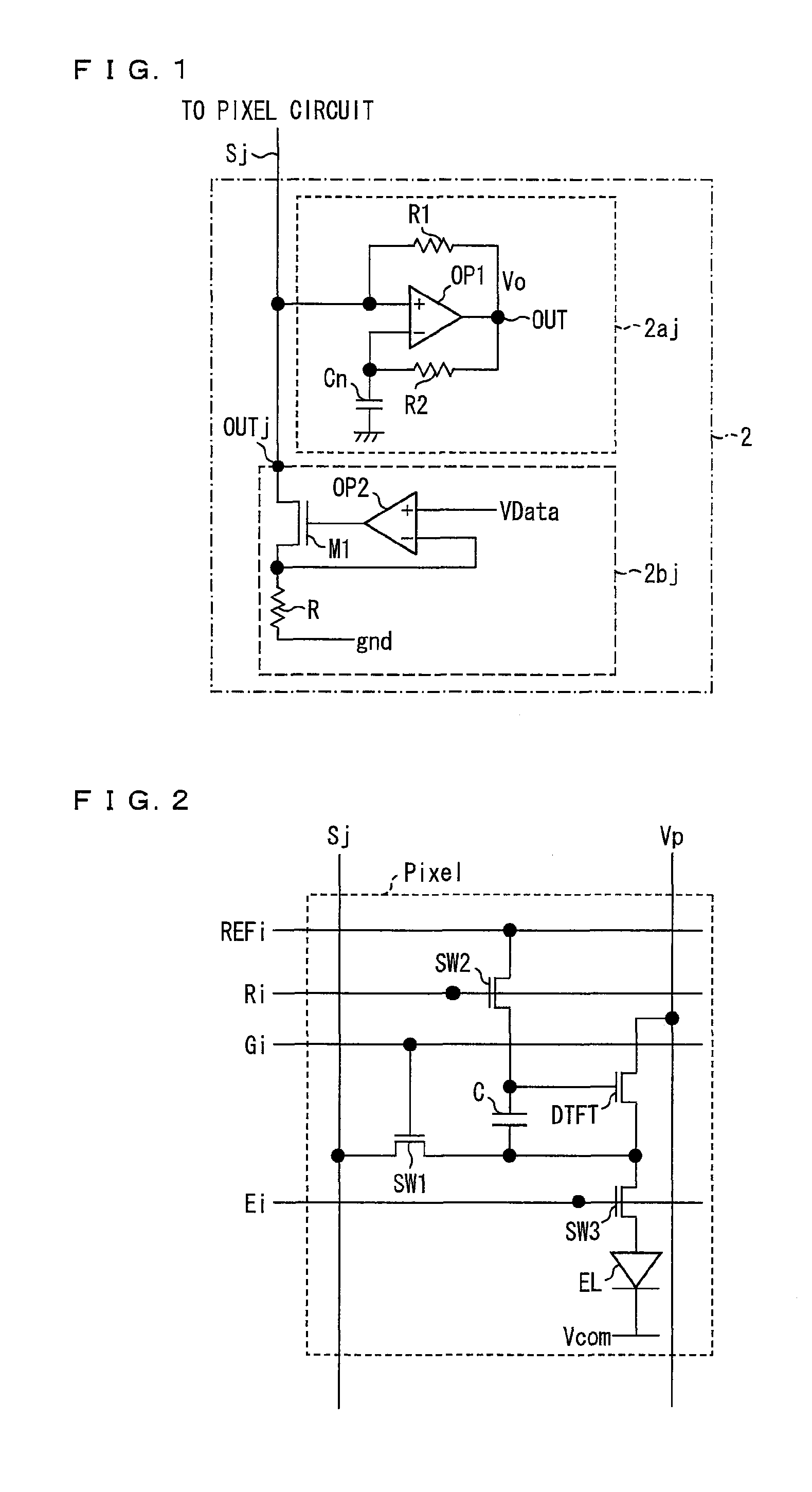
[0075]FIG. 1 illustrates how the output section of the source driver circuit 2 of the present embodiment is configured.

[0076]The output section includes, for each column (i.e., for each data signal line Sj), a negative capacitance circuit 2aj and a constant current circuit 2bj.

[0077]The negative capacitance circuit 2aj includes an operational amplifier OP1, resistors (resistor elements) R1 and R2, and a capacitor (capacitor element) Cn.

[0078]A non-inverting input terminal of the operational amplifier OP1 is connected with a corresponding data signal line Sj. Note here that, although the non-inverting input terminal is directly connected with the data signal line Sj, another element can be provided between the non-inverting input terminal and the data signal line Sj. Further, although the present embodiment describes with an example in which the operational amplifier OP1 is connected to each data signal line Sj, the operational amplifier OP1 can be connected only to one or each of s...

embodiment 2

[0101]FIG. 7 illustrates how an output section of the source driver circuit 2 of the present embodiment is configured.

[0102]The output section is different from the configuration of FIG. 1 in that the impedance element Z1 is a capacitor Cn, the impedance element Z2 is a resistor R2, and the impedance element Z3 is a resistor R1. The impedance element Z2 and the impedance element Z3 are resistor elements, which are of the same kind.

[0103]In this case, input impedance is represented, in the similar manner to Embodiment 1, by the following equation:

Zin=−((1 / jωCn) / R2)×R1

accordingly, the following negative capacitance is obtained:

Negative capacitance=−(R2 / R1)×Cn  (3)

[0104]In this case, a condition (condition of stability of a system) for achieving negative feedback is as follows:

|Zn|<|Zin|

that is,

Cp>(R2 / R1)×Cn

where, Zn is a value of total impedance of pixels electrically connected with a data signal line Sj, which impedance is obtained while the data signal line Sj and the pixels ele...

embodiment 3

[0108]FIG. 8 illustrates how an output section of the source driver circuit 2 of the present embodiment is configured.

[0109]The output section is different from the configuration of FIG. 1 in that the impedance element Z1 is a capacitor C1, the impedance element Z2 is a capacitor C2, and the impedance element Z3 is a capacitor Cn. The impedance element Z1 and the impedance element Z2 are capacitor elements, which are of the same kind. The impedance element Z2 and the impedance element Z3 are capacitor elements, which are of the same kind.

[0110]In this case, the following negative capacitance is obtained in the similar manner to Embodiment 1:

Negative capacitance=−(C1 / C2)×Cn  (5)

[0111]In this case, a condition (condition of stability of a system) for achieving negative feedback is as follows:

|Zn|<|Zin|

that is,

Cp>(C1 / C2)×Cn

where, Zn is a value of total impedance of pixels electrically connected with a data signal line Sj, which impedance is obtained while the data signal line Sj an...


PUM


Abstract

The present invention achieves a display device capable of quick compensation of charging of parasitic capacitance with a simple configuration and low power consumption. The display device in accordance with the present invention includes (i) pixels, (ii) signal wires (Sj), and (iii) an operational amplifier (OP1) having a non-inverting input terminal connected with a corresponding signal wire (Sj). The operational amplifier (OP1) is configured such that: the non-inverting input terminal is connected with an output terminal (OUT) via a first impedance element (R1); an inverting input terminal is connected with the output terminal (OUT) via a second impedance element (R2); and the inverting input terminal is connected with a reference voltage terminal via a third impedance element (Cn). A value Zn of total impedance of pixels electrically connected with the corresponding signal wire, which impedance is obtained while the corresponding signal wire and the pixels electrically connected with the corresponding signal wire are being supplied with an image signal, is represented by |Zn|<|Z1|·|Z3| / |Z2|, where Z1, Z2, and Z3 are values of impedance of the respective first through third impedance elements (R1, R2, and Cn).

Description

CROSS REFERENCE TO RELATED APPLICATIONS[0001]This is a U.S. National Phase patent application of PCT / JP2010 / 001395, filed Mar. 2, 2010, which claims priority to Japanese Patent Application No. 2009-116642, filed May 13, 2009, each of which is hereby incorporated by reference in the present disclosure in its entirety.TECHNICAL FIELD[0002]The present invention relates to a display device.BACKGROUND ART[0003]When driving a light emitting element (i.e., a current element) to be controlled by a supplied current, such as an organic EL or a light emitting diode, it is necessary to control a minute electric current supplied to the current element. Out of these, regarding the organic EL, with an increase in efficiency of the organic EL, it has been required to accurately and quickly control a minute current supplied to the organic EL especially in a hold mode.[0004]On the one hand there has been a large demand for lower power consumption and the efficiency of an organic EL element is expecte...

Claims


Application Information

Patent Timeline
Patent Type & Authority Patents(United States)
IPC IPC(8): G06F3/045H03F3/00G09G5/00G06F3/043G06F3/041G06F3/042G06F3/02H03F1/02G09G3/3216G09G3/3241G09G3/3266G09G3/3275G09G3/3283H05B44/00
CPCG09G2310/0254G09G3/3283G09G2310/0248G09G3/3233G09G2320/0252
Inventor KISHI, NORITAKA
Owner SHARP KK
Learn More