Electro-optical device and electronic apparatus

a technology applied in the field of optical devices and electronic devices, can solve the problems of consuming electric charges and causing electrostatic damage, and achieve the effect of improving reliability

Active Publication Date: 2014-08-12
SEIKO EPSON CORP
View PDF10 Cites 238 Cited by
  • Summary
  • Abstract
  • Description
  • Claims
  • Application Information

AI Technical Summary

Benefits of technology

[0023]According to this structure, because the electronic apparatus includes the foregoing electro-optical device, the transistors and the wiring lines, which are connected to the power supply wiring lines provided in peripheral circuitry, may be protected from static electricity, so that the electronic apparatus that allows improvement in the reliability and the yield thereof to be achieved may be provided.

Problems solved by technology

In the liquid crystal device, for example, due to static electricity generated in a manufacturing process, excessive voltage may be applied to transistors and wiring lines provided in peripheral circuitry (specifically, circuitry such as a data line driving circuit and a scanning line driving circuit which are connected to a power source), and thereby electrostatic damage is caused.
In the technique disclosed in JP-A-2007-65157, however, because the common wiring line is disposed on a layer that is above a layer on which the transistors, the wiring lines, and so forth are provided, and is connected to them, when patterning of the wiring lines and so forth is performed, the power supply wiring lines have not yet been connected to each other in an integrated manner.
Hence, if static electricity is generated when the patterning is performed, because there are no paths to let the static electricity escape, electric charges are concentrated in the transistors, the wiring lines, etc. and thereby damage them.
In addition, the electrical conductors may be used as inrush resistors and thereby may consume electric charges.

Method used


Image

  • Electro-optical device and electronic apparatus
  • Electro-optical device and electronic apparatus
  • Electro-optical device and electronic apparatus

Examples


first modification

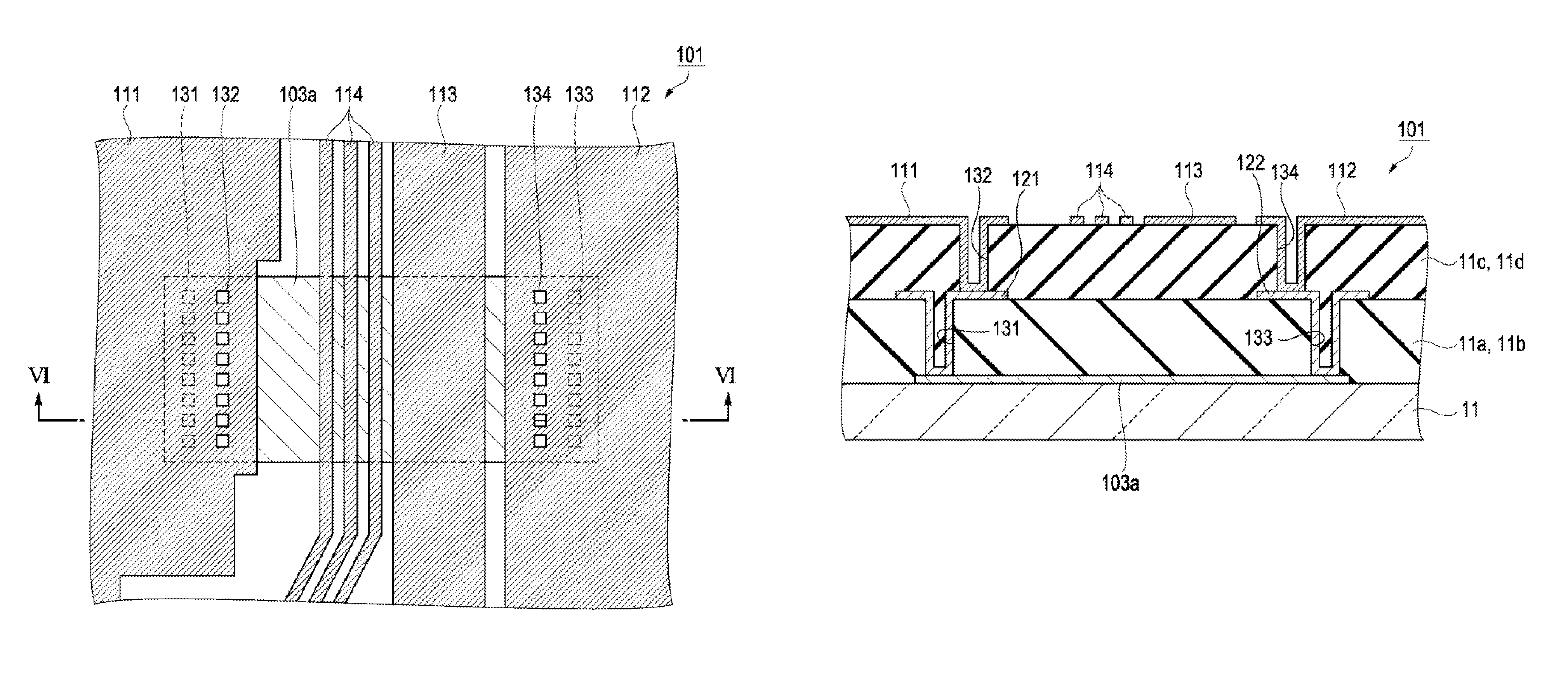
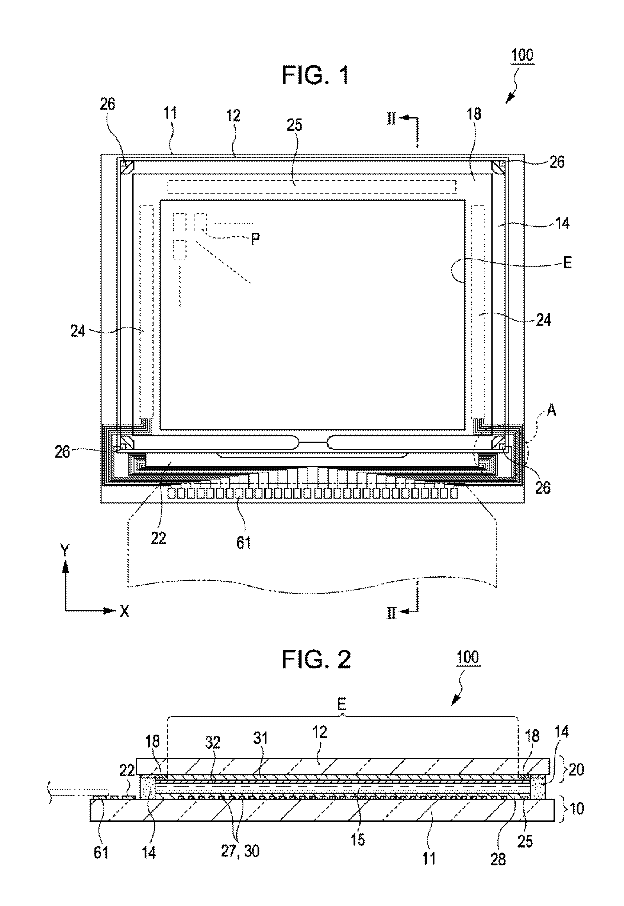
[0102]The structure of the electro-optical device is not limited to that of the foregoing liquid crystal device 100. As long as an electro-optical device includes power supply wiring lines, a first electrical conductor, a second electrical conductor, and a wiring line, and as long as the first electrical conductor, the second electrical conductor, and the wiring line are provided on layers below the power supply wiring lines, such a structure may be applied to an electro-optical device having another structure.

second modification

[0103]As described above, the first VDD power supply wiring line 111 and the second VDD power supply wiring line 112 are electrically connected to each other in an integrated manner (maintained at the same potential) by the common wiring line (contact hole, electrical conductor, and wiring line). Aspects of the invention are not limited to this. Other power supply wiring lines may be electrically connected to each other in an integrated manner. For example, a VSS power supply wiring line connected to the data line driving circuit 22 and a VSS power supply wiring line connected to the scanning line driving circuit 24 may be electrically connected to each other in an integrated manner using the common wiring line.

third modification

[0104]The foregoing electro-optical device is not limited to the liquid crystal device 100. Examples of the electro-optical device may include display devices, such as an organic electroluminescence (EL) device and an electrophoresis apparatus. Also, examples of the electro-optical device may include a reflective liquid crystal device (LCOS), a plasma display (PDP), a field emission display (FED, SED or the like), and a digital micromirror device (DMD).


PUM


Abstract

A liquid crystal device includes a scanning line driving circuit, a data line driving circuit, a first VDD power supply wiring line that supplies power to the data line driving circuit, a second VDD power supply wiring line that supplies power to the scanning line driving circuit, and a common wiring line that electrically connects the first VDD power supply wiring line and the second VDD power supply wiring line to each other in an integrated manner. The common wiring line includes electrical conductors, a wiring line, and contact holes.

Description

BACKGROUND[0001]1. Technical Field[0002]The present invention relates to an electro-optical device and an electronic apparatus.[0003]2. Related Art[0004]An active drive type liquid crystal device that includes transistors, which serve as elements for controlling switching of pixel electrodes, corresponding to pixels is a known example of an electro-optical device. In the liquid crystal device, for example, due to static electricity generated in a manufacturing process, excessive voltage may be applied to transistors and wiring lines provided in peripheral circuitry (specifically, circuitry such as a data line driving circuit and a scanning line driving circuit which are connected to a power source), and thereby electrostatic damage is caused.[0005]JP-A-2007-65157, for example, discloses a technique in which a power supply wiring line for a data line driving circuit and a power supply wiring line for a scanning line driving circuit are connected to each other in an integrated manner ...

Claims


Application Information

Patent Timeline
Patent Type & Authority Patents(United States)
IPC IPC(8): G09G5/00G06F3/038
CPCG02F1/1345G02F1/13G02F2001/13456G09G3/36G02F1/13454G09G3/20G09G2330/04G02F1/13456
Inventor OIKAWA, HIROYUKI
Owner SEIKO EPSON CORP
Why Eureka
Try Eureka