AI technical title is built by Patsnap AI team. It summarizes the technical point description of the patent document.
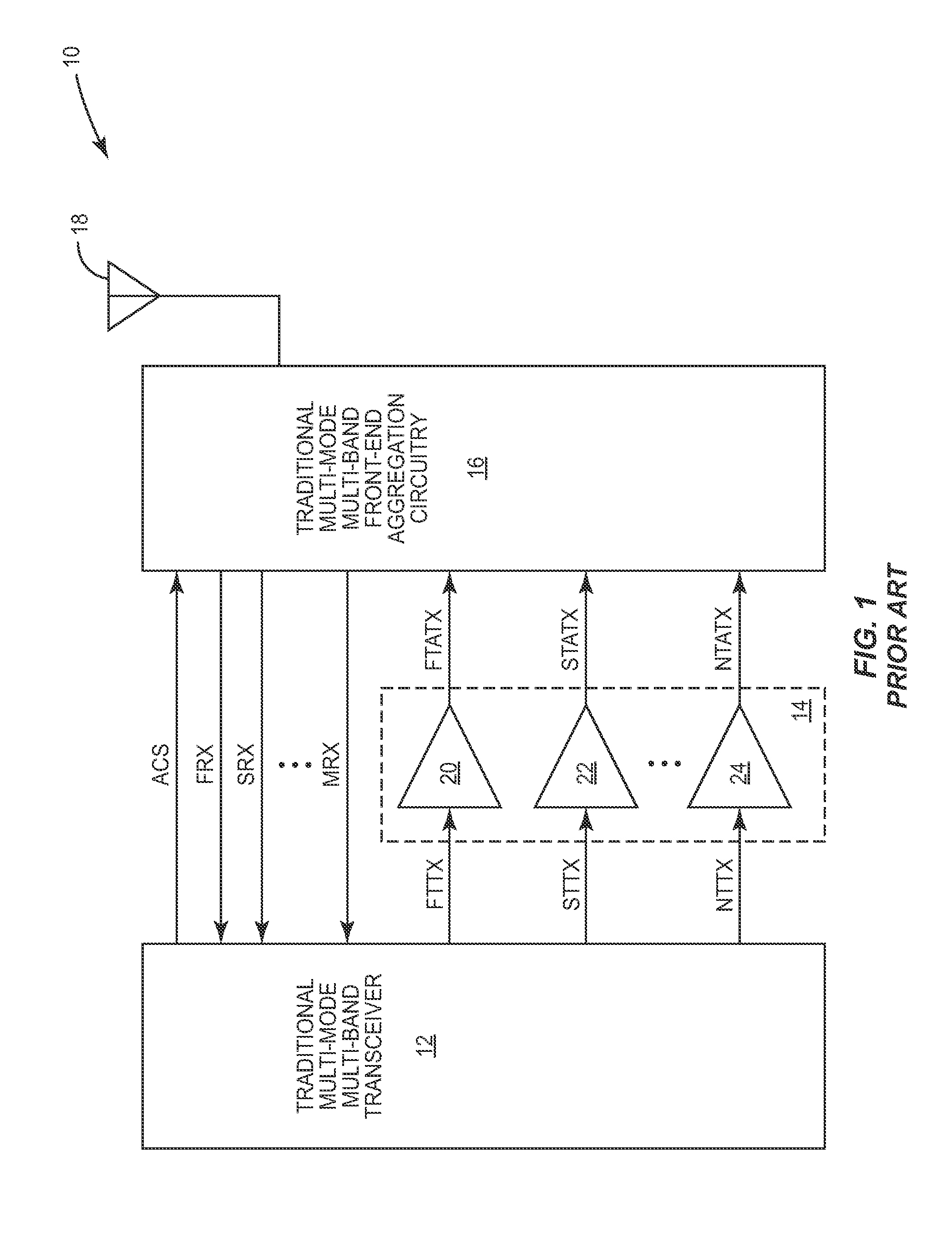
a technology of semiconductor die structure and converter, which is applied in the direction of gated amplifier, process and machine control, instruments, etc., can solve the problem that the receiver in such a transceiver does not operate simultaneously, and achieve the effect of reducing noise and potential interference, and minimizing the length of the transient current path
Active Publication Date: 2014-08-19
QORVO US INC
View PDF231 Cites 7 Cited by
Summary
Abstract
Description
Claims
Application Information
AI Technical Summary
This helps you quickly interpret patents by identifying the three key elements:
Problems solved by technology
Method used
Benefits of technology
Benefits of technology
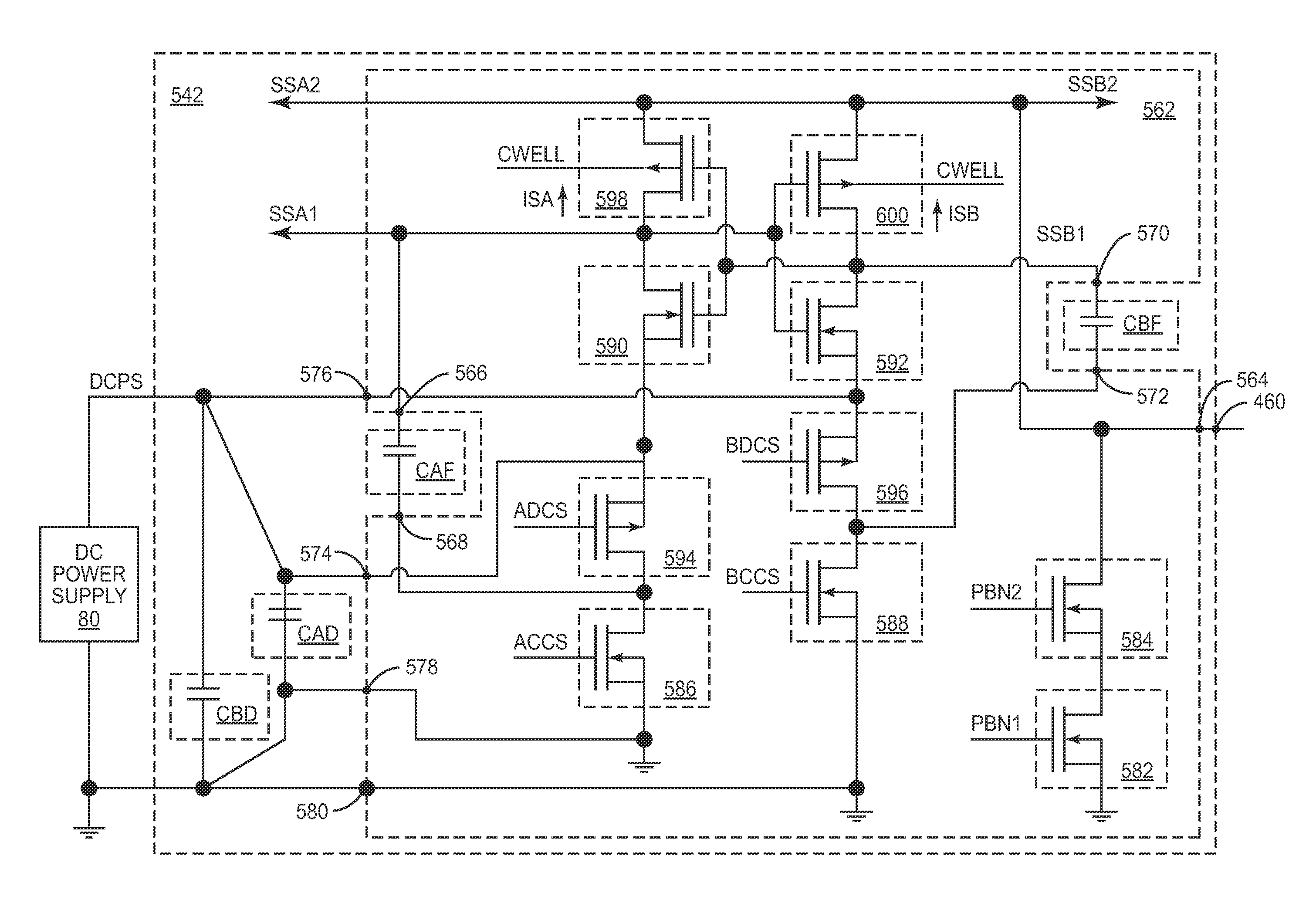
[0016]The present disclosure relates to a DC-DC converter having a DC-DC converter semiconductor die and an alpha flying capacitive element. The DC-DC converter semiconductor die includes a first series alpha switching element, a second series alpha switching element, a first alpha flying capacitor connection node, which is about over the second series alpha switching element, and a second alpha flying capacitor connection node, which is about over the first series alpha switching element. The alpha flying capacitive element is electrically coupled between the first alpha flying capacitor connection node and the second alpha flying capacitor connection node. By locating the first alpha flying capacitor connection node and the second alpha flying capacitor connection node about over the second series alpha switching element and the first series alpha switching element, respectively, lengths of transient current paths may be minimized, thereby reducing noise and potential interference.
Problems solved by technology
Therefore, the transmitter and receiver in such a transceiver do not operate simultaneously.
Method used
Image
Click on the blue label to locate the original text in one second.
Reading with bidirectional positioning of images and text.
Examples
first embodiment
[0152]FIG. 131B shows the SAH current estimating circuit and the series switching element according to the SAH current estimating circuit and the series switching element.
second embodiment
[0153]FIG. 131C shows the SAH current estimating circuit and the series switching element according to the SAH current estimating circuit and the series switching element.
third embodiment
[0154]FIG. 131D shows the SAH current estimating circuit and the series switching element according to the SAH current estimating circuit and the series switching element.
[0155]FIG. 132 shows details of the SAH current estimating circuit illustrated in FIG. 131A according to one embodiment of the SAH current estimating circuit.
[0156]FIG. 133 shows a process for preventing undershoot disruption of a bias power supply signal illustrated in FIG. 44 according to one embodiment of the present disclosure.
[0157]FIG. 134 shows a process for optimizing efficiency of a charge pump illustrated in FIG. 44 according to one embodiment of the present disclosure.
[0158]FIG. 135 shows a process for preventing undershoot of the PA envelope power supply illustrated in FIG. 43 according to one embodiment of the present disclosure.
[0159]FIG. 136 shows a process for selecting a converter operating mode of the PA envelope power supply according to one embodiment of the present disclosure.
[0160]FIG. 137 sho...
PUM
Abstract
A direct current (DC)-DC converter having a DC-DC converter semiconductor die and an alpha flying capacitive element is disclosed. The DC-DC converter semiconductor die includes a first series alpha switching element, a second series alpha switching element, a first alpha flying capacitor connection node, which is about over the second series alpha switching element, and a second alpha flying capacitor connection node, which is about over the first series alpha switching element. The alpha flying capacitive element is electrically coupled between the first alpha flying capacitor connection node and the second alpha flying capacitor connection node. By locating the first alpha flying capacitor connection node and the second alpha flying capacitor connection node about over the second series alpha switching element and the first series alpha switching element, respectively, lengths of transient current paths may be minimized, thereby reducing noise and potential interference.
Description
PRIORITY CLAIMS[0001]The present application claims priority to U.S. Provisional Patent Application No. 61 / 410,071, filed Nov. 4, 2010.[0002]The present application claims priority to U.S. Provisional Patent Application No. 61 / 417,633, filed Nov. 29, 2010.[0003]The present application claims priority to and is a continuation-in-part of U.S. patent application Ser. No. 13 / 090,663, filed Apr. 20, 2011, entitled “QUADRATURE POWER AMPLIFIER ARCHITECTURE,” now U.S. Pat. No. 8,538,355, which claims priority to U.S. Provisional Patent Applications No. 61 / 325,859, filed Apr. 20, 2010; No. 61 / 359,487, filed Jun. 29, 2010; No. 61 / 370,554, filed Aug. 4, 2010; No. 61 / 380,522, filed Sep. 7, 2010; No. 61 / 410,071, filed Nov. 4, 2010; and No. 61 / 417,633, filed Nov. 29, 2010.[0004]The present application claims priority to and is a continuation-in-part of U.S. patent application Ser. No. 13 / 172,371, filed Jun. 29, 2011, entitled “AUTOMATICALLY CONFIGURABLE 2-WIRE / 3-WIRE SERIAL COMMUNICATIONS INTERFA...
Claims
Application Information
Patent Timeline
Application Date:The date an application was filed.
Publication Date:The date a patent or application was officially published.
First Publication Date:The earliest publication date of a patent with the same application number.
Issue Date:Publication date of the patent grant document.
PCT Entry Date:The Entry date of PCT National Phase.
Estimated Expiry Date:The statutory expiry date of a patent right according to the Patent Law, and it is the longest term of protection that the patent right can achieve without the termination of the patent right due to other reasons(Term extension factor has been taken into account ).
Invalid Date:Actual expiry date is based on effective date or publication date of legal transaction data of invalid patent.
InventorDEUCHARS, ROBERTBERCHTOLD, JEAN-CHRISTOPHECOLLES, JOSEPH HUBERTZIMLICH, DAVIDLEVESQUE, CHRISSOUTHCOMBE, WILLIAM DAVIDJONES, DAVID E.YODER, SCOTTSTOCKERT, TERRY J.

