
Touch sensor panel

a sensor panel and touch technology, applied in the field of touch sensor panels, can solve the problems of reducing current or voltage, difficult to recognize an object having a small area during a touch operation, and difficulty in increasing the degree of completion of products using only input devices, so as to minimize parasitic capacitance, minimize parasitic capacitance, and maximize the contour line of the sensing layer

Inactive Publication Date: 2014-09-02
DONGBU HITEK CO LTD
View PDF14 Cites 16 Cited by
  • Summary
  • Abstract
  • Description
  • Claims
  • Application Information

AI Technical Summary

Benefits of technology

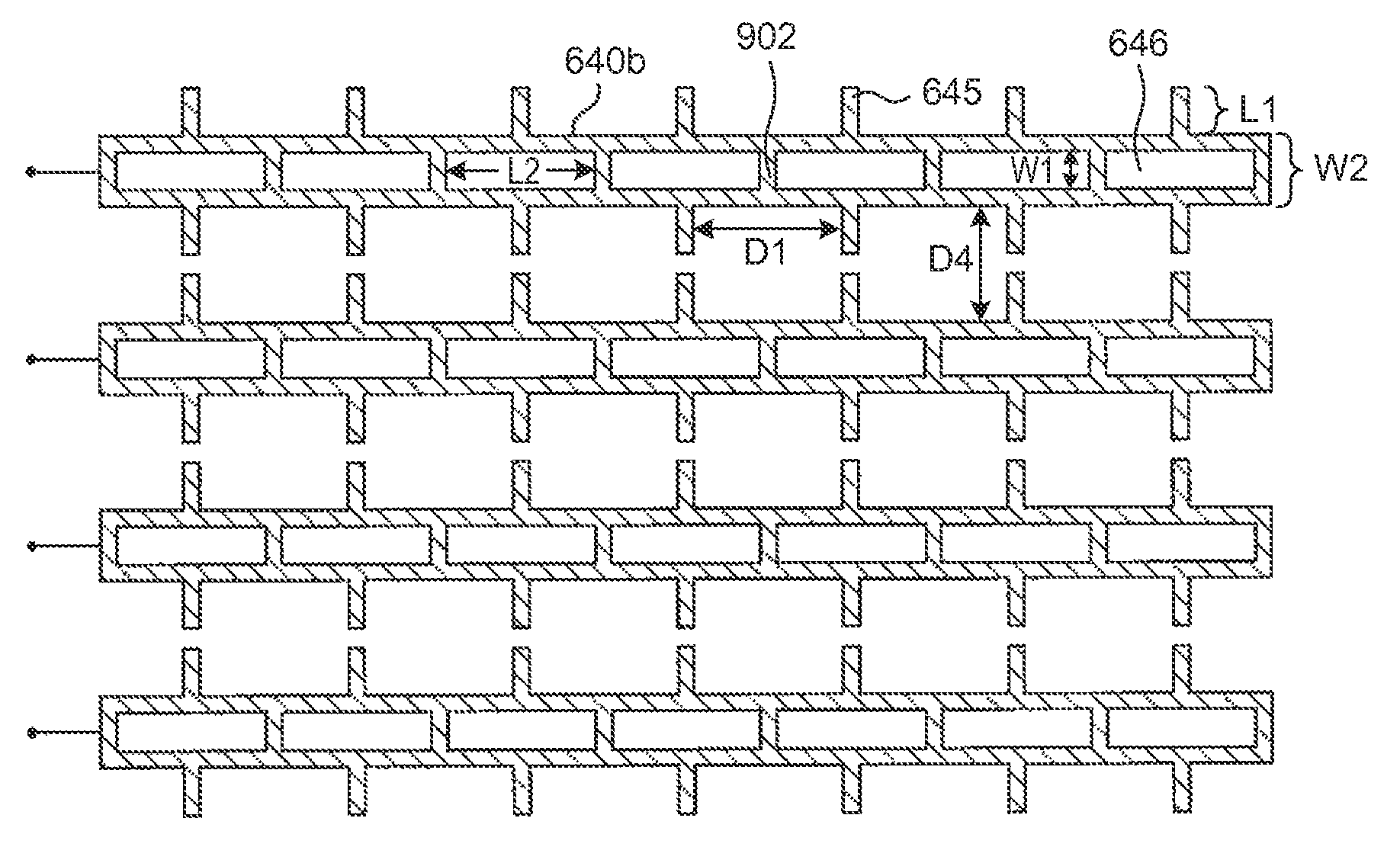
[0013]In view of the above, the present invention provides a two-layer mutual type touch sensor panel that measures mutual capacitance between a sensing layer and a driving layer to sense a touch operation, provides various sensing layer patterns capable of maximizing the contour line of the sensing layer and reducing an empty space area (e.g., an opening) in the central portion of a sensing layer pattern, and when a user touches the surface of a touch sensor panel (e.g., in a display unit) with his / her body part, such as his / her finger, minimizes parasitic capacitance between the body part, such as the finger, and the sensing layer of the touch sensor panel to more accurately measure mutual capacitance between the sensing layer and the driving layer, thereby increasing sensing accuracy.
[0027]The present two-layer mutual type touch sensor panel measures mutual capacitance between the sensing layer and the driving layer to sense a touch operation, and provides various sensing layer patterns capable of maximizing the contour line of the sensing layer and reducing an area that may cause parasitic capacitance with a human body by forming an empty space or opening in the central portion of the sensing layer pattern. Accordingly, when a user touches the surface of a display unit of a touch sensor panel with his / her body part, such as his / her finger, it is possible to minimize parasitic capacitance between the body part, such as the finger, and the sensing layer of the touch sensor panel to more accurately measure mutual capacitance between the sensing layer and the driving layer, thereby increasing sensing accuracy.
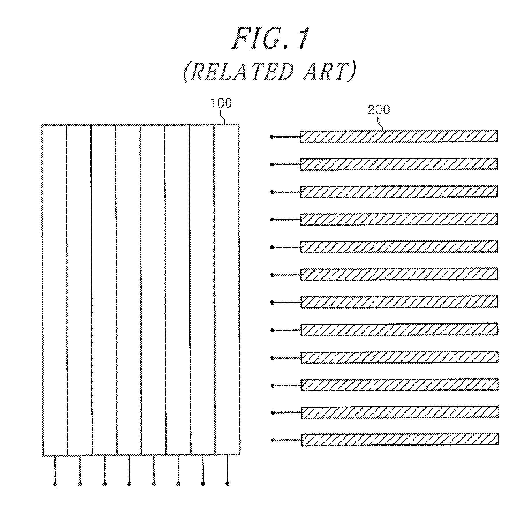
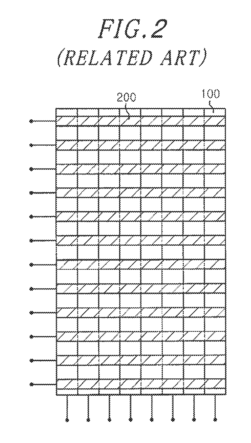
[0028]In regard to the sensing layer pattern, since various patterns in which one or more empty spaces or openings are formed in the central portion of the bar pattern, it is possible to narrow the interval between the sensing layers while minimizing parasitic capacitance compared to the bar pattern of the related art, thereby reducing the minimum touch area. It is also possible to decrease the resistances of the sensing layer and the driving layer, making it possible to more accurately measure the mutual capacitance between the sensing layer and the driving layer.

Problems solved by technology

With the increasing development of mobile communication equipment, it is difficult to increase the degree of completion of products using only input devices, such as a keyboard and a mouse.
However, there is a problem in that a resistance component increases, causing a decrease in a current or voltage resulting from mutual capacitance.
If the width of the sensing layer 200 is excessively small, as shown in FIG. 5, the minimum area between the sensing layers for recognizing the body part expands, making it difficult to recognize an object having a small area during a touch operation.

Method used


Image

  • Touch sensor panel
  • Touch sensor panel
  • Touch sensor panel

Examples


Embodiment Construction

[0040]Hereinafter, operation of the invention will be described in detail with reference to the accompanying drawings. In the following description of the present invention, a detailed description of the already known structures and operations may confuse the subject matter of the present invention, and therefore, the detailed description thereof will be omitted. The following terms have been defined by considering functions in the embodiments of the present invention and may be changed for the invention and practice. Hence, the terms may be defined throughout the description of the present invention.

[0041]FIG. 6 shows the structure of a two-layer mutual type touch sensor panel in accordance with an embodiment of the invention. Further, an insulating material 650 is interposed between the driving layer 630 and sensing layer 640.

[0042]Referring to FIG. 6, a touch sensor panel 600 has a lower insulating sheet 610 and an upper insulating sheet 620 that are bonded to each other at a pre...


PUM


Abstract

A touch sensor panel includes at least one first electrode, and a second electrode above the at least one first electrode configured to cross the at least one first electrode, and having one or more openings therein.

Description

RELATED APPLICATIONS[0001]This application claims the benefit of Korean Patent Application No. 10-2011-0083916, filed on Aug. 23, 2011, which is hereby incorporated by reference as if fully set forth here in.FIELD OF THE INVENTION[0002]The present invention relates to a touch sensor panel. In particular, the present invention relates to a two-layer mutual type touch sensor panel that measures mutual capacitance between a sensing layer and a driving layer to sense touch, presents various sensing layer patterns capable of maximizing the contour line of the sensing layer where mutual capacitance changes due to an external object and reducing the area of empty space in the central portion of the sensing layer pattern. When a user touches the surface of a display unit of a touch sensor panel with his / her body part, such as his / her finger, parasitic capacitance between the body part, such as the finger, and the sensing layer of the touch sensor panel is minimized to more accurately measur...

Claims


Application Information

Patent Timeline
Patent Type & Authority Patents(United States)
IPC IPC(8): G09G5/00G06F3/041G06F3/044
CPCG06F3/0416G06F3/044G06F3/0446G06F3/0448G06F3/0445G06F2203/04111
Inventor HONG, WONCHEOL
Owner DONGBU HITEK CO LTD
Learn More