Integrated circuit

a technology of integrated circuits and bond wires, applied in the field of integrated circuits, can solve the problems of complex fabrication of multiple parallel layers of bond wires, poor power transfer, and large inductance of bond wires, and achieve the effect of maximising the power transfer of high frequency signals

Inactive Publication Date: 2014-09-09
SONY CORP
View PDF4 Cites 0 Cited by
  • Summary
  • Abstract
  • Description
  • Claims
  • Application Information

AI Technical Summary

Benefits of technology

[0005]A first aspect of the invention is defined in claim 1. By providing the conductive ribbon having the main portion which continuously increases in width, a desired characteristic impedance of the conductive ribbon may match the characteristic impedance of both the die and the substrate. Advantageously an impedance matching structure may be provided for the integrated circuit, to maximise power transfer of high frequency signals across the integrated circuit.
[0006]A second aspect of the invention is defined in claim 2. By providing the ground plane having the first aperture immediately adjacent to the conductive ribbon, a desired characteristic impedance of the conductive ribbon may match the characteristic impedance of both the die and the substrate. Advantageously an impedance matching structure may be provided for the integrated circuit, to maximise power transfer of high frequency signals across the integrated circuit.

Problems solved by technology

However, some bond wires may have large inductances due to their long and thin structures.
This poses a challenge when transmitting high frequency signals in the integrated circuit, since large inductance may lead to poor power transfer.
However, a problem with this arrangement of the bond wires 101 is the complexity in fabricating the multiple parallel layers of the bond wires 101, where the gaps between the adjacent bond wires 101 have to be strictly controlled.

Method used


Image

  • Integrated circuit
  • Integrated circuit
  • Integrated circuit

Examples


Embodiment Construction

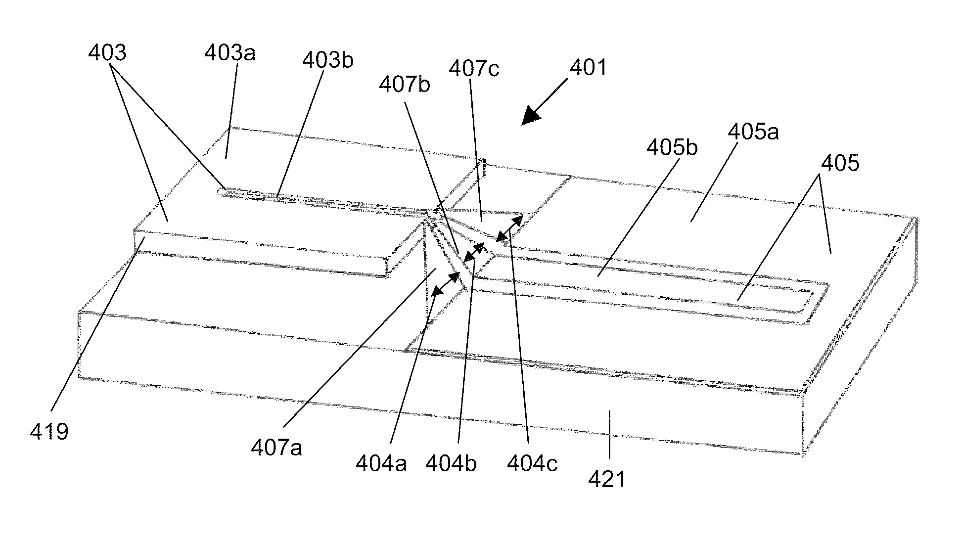
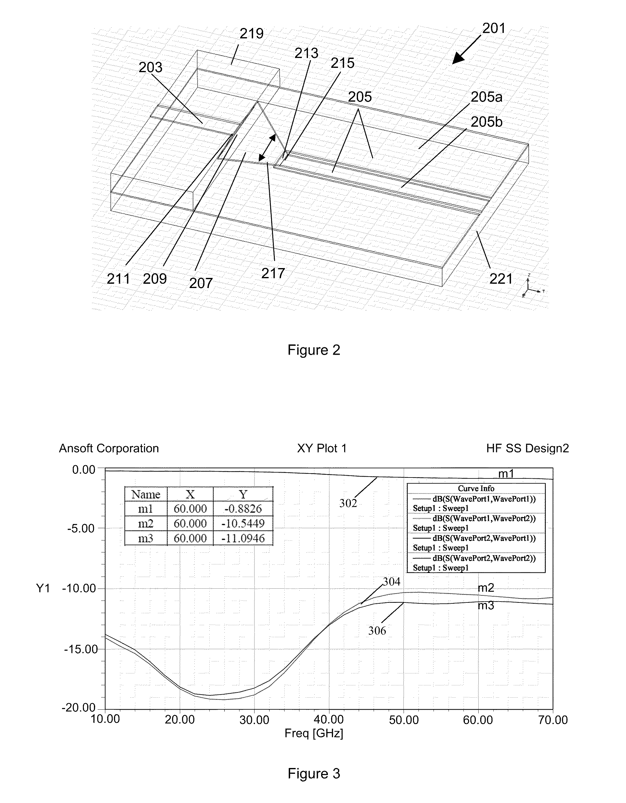
[0018]Example embodiments may be used in a high frequency integrated circuit. The transmission lines in the high frequency integrated circuit may include a microstrip line assembly and / or a coplanar waveguide. The microstrip line assembly has three layers: a microstrip line, a dielectric substrate layer (which may be a semiconductor die), a ground plane. The co-planar waveguide has two layers: a conductive strip spaced from a coplanar ground plane, and a substrate. A grounded co-planar waveguide has an additional ground plane beneath the substrate.

[0019]Several example embodiments will now be described including:[0020]a) a first embodiment to couple a microstrip line assembly to a stepwise co-planar waveguide via a conductive ribbon having a varying width, where both transmission lines have the same impedance,[0021]b) a second embodiment to couple a co-planar waveguide to a stepwise co-planar waveguide via conductive ribbons each having a varying width, where both transmission lines...


PUM


Abstract

An integrated circuit connection comprises a substrate, first and second transmission lines, a die, and a conductive ribbon. The first transmission line has a first end and is arranged on the substrate. The die is spaced from the first end. The die has a first surface, which is arranged on the substrate, and a second surface, which is opposite to the first surface and which has the second transmission line arranged thereon. The second transmission line has a second end. The conductive ribbon electrically couples the first and the second ends.

Description

CROSS REFERENCE TO RELATED APPLICATIONS[0001]The present application claims priority to Singapore Patent Application JP 200905424-8 filed in the Singapore Patent Office on Aug. 12, 2009, the entire contents of which is incorporated herein by reference.FIELD OF THIS INVENTION[0002]This invention relates to an integrated circuit.BACKGROUND OF THE INVENTION[0003]In the prior art, it is known to use bond wires to connect components in an integrated circuit. Bond wires may be inexpensive and may also account for thermal expansion for reliability. However, some bond wires may have large inductances due to their long and thin structures. This poses a challenge when transmitting high frequency signals in the integrated circuit, since large inductance may lead to poor power transfer.[0004]In U.S. Pat. No. 4,686,492 (‘Grellmann’), multiple parallel layers of bond wires 101 are connected between different transmission lines 103, 105 in an integrated circuit 100; see FIG. 1. Such an arrangement...

Claims


Application Information

Patent Timeline
Patent Type & Authority Patents(United States)
IPC IPC(8): H01L29/93
CPCH01L24/48H01L23/66H01L24/49H01L24/50H01L2223/6611H01L2223/6627H01L2224/05553H01L2224/45012H01L2224/45014H01L2224/48095H01L2224/48465H01L2224/49111H01L2224/49174H01L2224/49175H01L2924/01005H01L2924/01006H01L2924/01023H01L2924/01027H01L2924/01033H01L2924/01074H01L2924/01082H01L2924/014H01L2924/14H01L2924/1903H01L2924/19033H01L2924/30107H01L2924/3011H01L2924/30111H01L2924/181H01L2924/00014H01L2224/49052H01L2924/00H01L2224/48227H01L2924/00012H01L2224/45099H01L2224/85399H01L2224/05599H01L2924/206
Inventor SUN, XIAOBINGZHANG, YAQIONGMA, YUGANG
Owner SONY CORP
Why Eureka
Try Eureka