Optical semiconductor lighting apparatus

Inactive Publication Date: 2014-09-23
POSCO LED
View PDF11 Cites 9 Cited by
  • Summary
  • Abstract
  • Description
  • Claims
  • Application Information

AI Technical Summary

Benefits of technology

[0010]The present invention has been made in an effort to solve the above problems, and provides an optical semiconductor lighti

Problems solved by technology

However, such a sealing member contracts or expands according to external environme

Method used


Image

  • Optical semiconductor lighting apparatus
  • Optical semiconductor lighting apparatus
  • Optical semiconductor lighting apparatus

Examples


Example

[0028]Exemplary embodiments of the present invention will be described below in detail with reference to the accompanying drawings. Throughout the disclosure, like reference numerals refer to like parts throughout the drawings and embodiments of the present invention.

[0029]Hereinafter, exemplary embodiments of the present invention will be described with reference to the accompanying drawings.

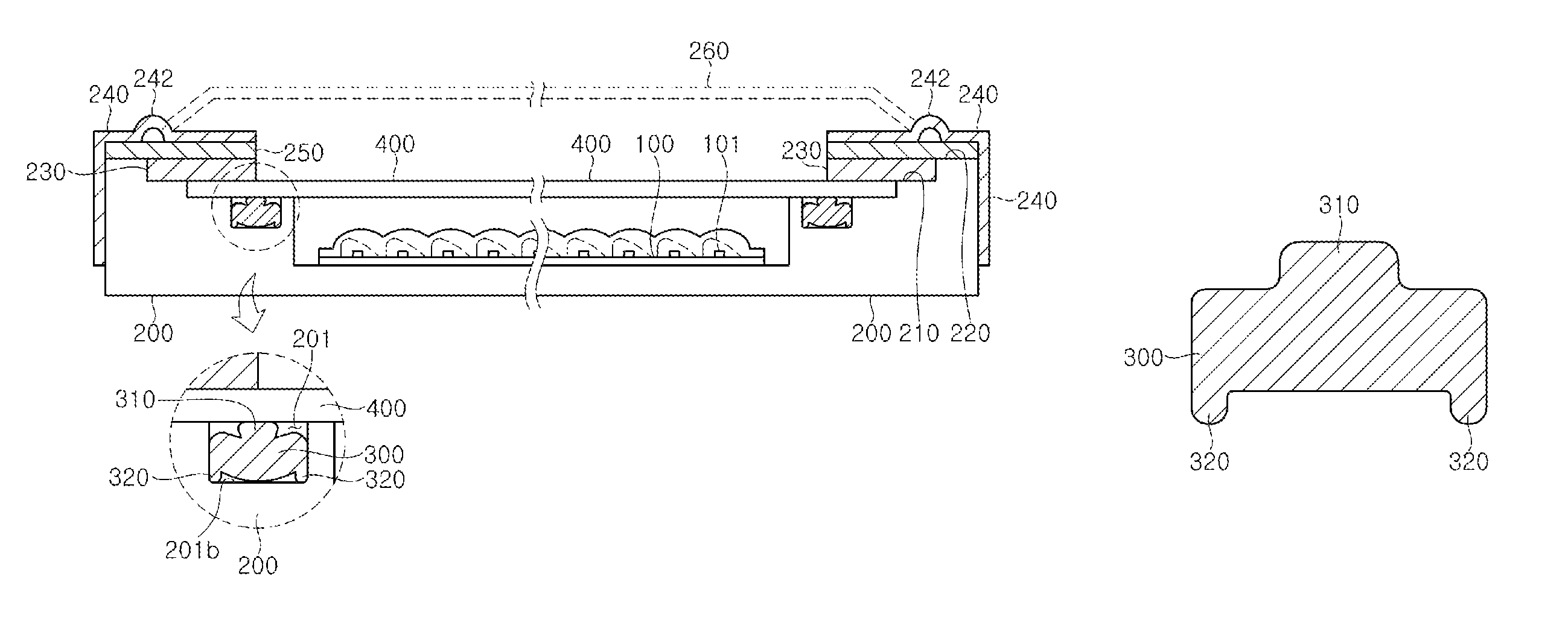
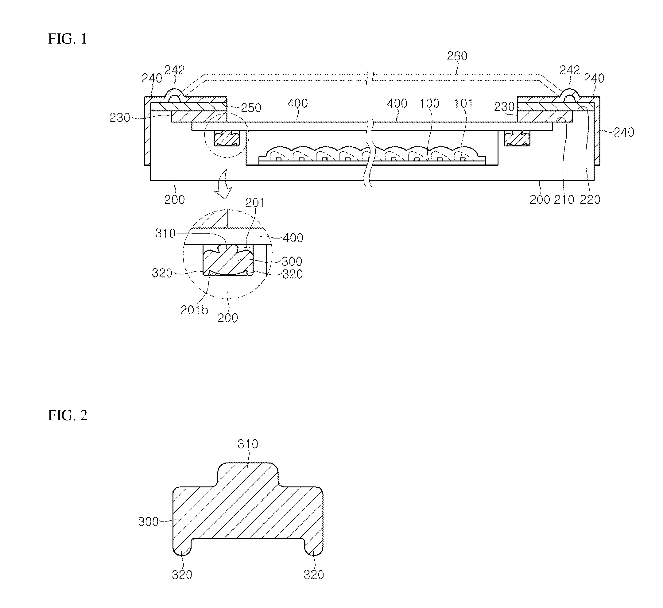
[0030]FIG. 1 is a cross-sectional conceptual diagram illustrating an overall configuration of an optical semiconductor lighting apparatus according to an embodiment of the present invention, and FIG. 2 is a cross-sectional conceptual diagram illustrating pre-modification states of a first sealing body and first and second ribs, which are essential components of the optical semiconductor lighting apparatus according to the embodiment of the present invention.

[0031]As illustrated in FIGS. 1 and 2, the optical semiconductor lighting apparatus includes a light emitting module 100, a housing 200, a ...


PUM


Abstract

An optical semiconductor lighting apparatus includes a light emitting module including a semiconductor optical device, a housing to house the light emitting module, a first sealing body connected to a groove recessed in a polygonal or closed-curve shape of the housing, a first optical cover covering an outer edge of the groove and a top surface of the housing, a first rib formed on a top surface of the first sealing body along a forming direction of the first sealing body, and a pair of second ribs formed in parallel along both edges of a bottom surface of the first sealing body.

Description

CROSS-REFERENCE(S) TO RELATED APPLICATION[0001]This application claims priority from and the benefit of Korean Patent Application No. 10-2013-0049419, filed on May 2, 2013, which is incorporated herein by reference for all purposes as if fully set forth herein.BACKGROUND[0002]1. Field[0003]The present invention relates to an optical semiconductor lighting apparatus, and more particularly, to an optical semiconductor lighting apparatus that can prevent penetration of moisture, particles, dust or the like and can improve the durability and connectivity thereof in its entirety.[0004]2. Discussion of the Background[0005]As compared with incandescent bulbs and fluorescent lamps, optical semiconductors using a light source, such as a light emitting diode (LED), an organic LED, a laser diode, and an organic electroluminescent diode, have low power consumption, long lifespan, superior durability, and high luminance. Due to these advantages, the optical semiconductors have recently attracted...

Claims


Application Information

Patent Timeline
IPC IPC(8): H01L29/22H01L29/24H01L33/00H01L29/227H01L33/52H01L33/58
CPCH01L33/52H01L33/58H01L33/483F21K9/00F21S8/02F21V3/00F21V15/01F21V31/005F21Y2101/02H01L33/54F21Y2115/10
Inventor KIM, JI WANKIM, YUN HAKIM, JUNG HWA
Owner POSCO LED
Why Eureka
Try Eureka