Optical writing control device, image forming apparatus, and optical writing control method for controlling the light emitting timing of a light source

a technology of optical writing and control device, which is applied in the direction of digitally marking record carriers, image enhancement, instruments, etc., can solve the problems of useless line memory which is not used, and the control device is not efficient to produ

Inactive Publication Date: 2014-09-30
RICOH KK
View PDF10 Cites 6 Cited by
  • Summary
  • Abstract
  • Description
  • Claims
  • Application Information

AI Technical Summary

Benefits of technology

[0015]An optical writing control device forms electrostatic latent images on image carriers by controlling light sources exposing the image carriers. The optical writing control device includes: a pixel information obtaining unit which obtains pixel information about pixels constituting an image which is to be formed and output, from a control unit of an image forming apparatus main body, and stores the pixel information in a storage medium; a light emission control unit which controls light emission of each of the multiple light sources which are provided for respective different colors, on the basis of the obtained information about the pixels, and exposes the multiple image carriers which are provided for the respective different colors; a detection signal obtaining unit which obtains a detection signal of a sensor that detects an image in a conveying path on which the image obtained by developing the electrostatic latent images formed on the image carriers is transferred and conveyed; a detection timing obtaining unit which obtains, on the basis of the obtained detection signal, detection timing of a positional deviation correction pattern used to correct a positional deviation in a sub-scanning direction between the different colors of the image that is formed by developing the electrostatic latent images formed using the multiple image carriers; a positional deviation amount obtaining unit which obtains a positional deviation amount in the sub-scanning direction for each of the different colors, on the basis of a difference between a reference value determined in advance and the detection timing of the positional deviation correction pattern obtained for a corresponding color; and a correction amount calculating unit which calculates a central value of a distribution range of the positional deviation amounts in the sub-scanning direction obtained for the different colors, and calculates a correction amount for each of the different colors on the basis of a difference between the calculated central value and the positional deviation amount in the sub-scanning direction obtained for a corresponding color. The light emission control unit controls light emission of each of the multiple light sources on the basis of the calculated correction amount of each of the different colors. When a correction amount indicates that light emitting timing of a light source is to be delayed, the light emission control unit delays the light emitting timing of the light source by delaying reading timing of the pixel information stored in the storage medium. When a correction amount indicates that light emitting timing of a light source for a color is to be advanced, the light emission control unit delays timing at which the pixel information about colors other than the color starts to be obtained from the control unit of the image forming apparatus main body, thus relatively advancing the light emitting timing of the light source for the color.
[0017]An optical writing control method forms electrostatic latent images on image carriers by controlling light sources exposing the image carriers. The optical writing control method includes: obtaining a detection signal of a sensor that detects an image, in a conveying path on which the image obtained by developing the electrostatic latent images formed on the image carriers is transferred and conveyed; obtaining, on the basis of the obtained detection signal, detection timing of a positional deviation correction pattern used to correct a positional deviation in a sub-scanning direction between different colors of the image that is formed by developing the electrostatic latent images formed on the multiple image carriers provided for the different colors; obtaining a positional deviation amount in the sub-scanning direction for each of the different colors, on the basis of a difference between a reference value determined in advance and the detection timing of the positional deviation correction pattern obtained for a corresponding color; and calculating a central value of a distribution range of the positional deviation amounts in the sub-scanning direction obtained for the different colors, and calculates a correction amount for each of the different colors on the basis of a difference between the calculated central value and the positional deviation amount in the sub-scanning direction obtained for a corresponding color. When a correction amount indicates that light emitting timing of a light source is to be delayed, the light emitting timing of the light source is delayed by delaying reading timing of pixel information stored in the storage medium used to obtain and store pixel information about pixels constituting the image which is to be formed and output. When the correction amount indicates that light emitting timing of a light source for a color is to be advanced, timing at which the pixel information about colors other than the color starts to be stored in the storage medium is delayed, and thus the light emitting timing of the light source for the color is relatively advanced.

Problems solved by technology

Here, the control devices of the colors need different number of lines in the line memory as described above, but it is not efficient to produce the control devices in accordance with the needed number of lines, and therefore, in many cases, it is common to provide a control device having a line memory for a number of lines with which a certain amount of shift can be made.
As a result, depending on the amount of shift of each color, there may be useless line memories which are not used.

Method used


Image

  • Optical writing control device, image forming apparatus, and optical writing control method for controlling the light emitting timing of a light source
  • Optical writing control device, image forming apparatus, and optical writing control method for controlling the light emitting timing of a light source
  • Optical writing control device, image forming apparatus, and optical writing control method for controlling the light emitting timing of a light source

Examples


Embodiment Construction

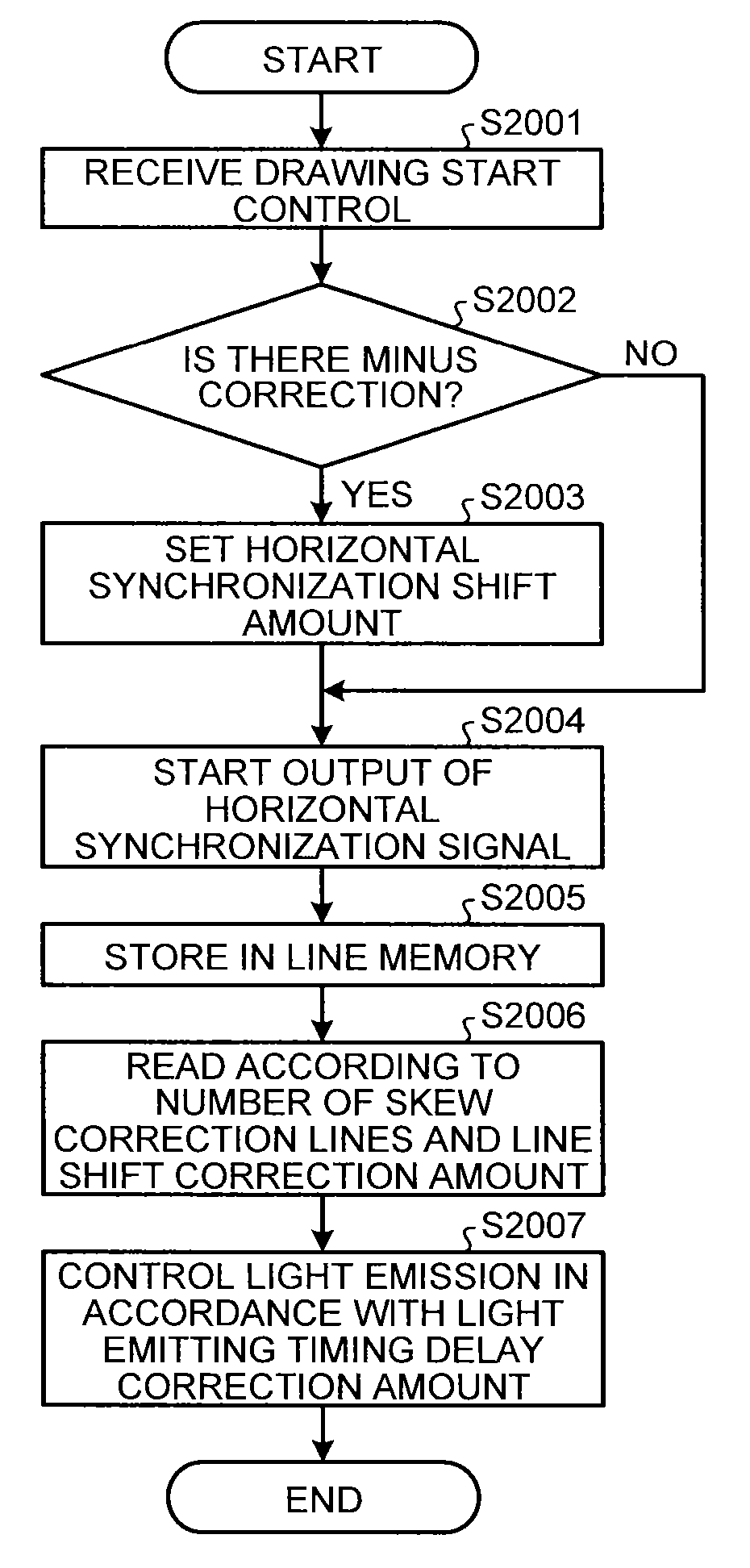
[0039]Hereinafter, an embodiment of the present invention will be explained in detail with reference to drawings. In the present embodiment, an image forming apparatus serving as a multifunction peripheral (MFP) will be explained as an example. The image forming apparatus according to the present embodiment is an electrophotography image forming apparatus, and the gist thereof is detailed processing for adjusting a position in a sub-scanning direction where a toner image developed on a photosensitive element serving as an image carrier is transferred.

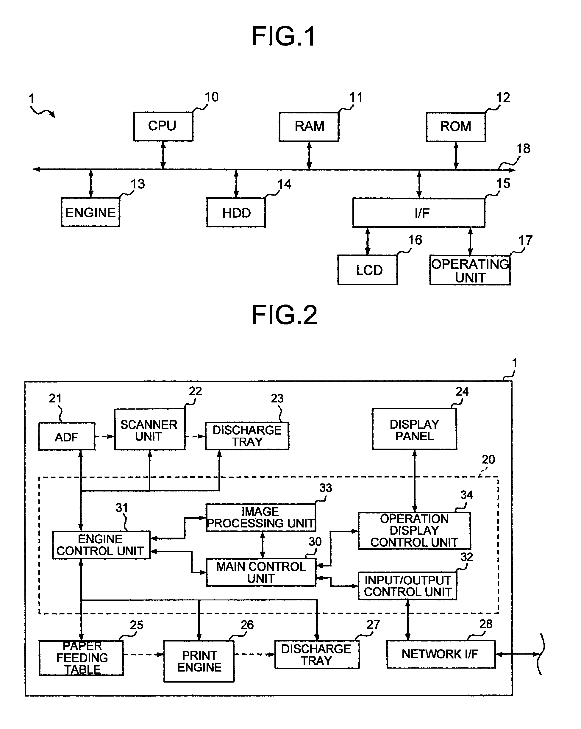
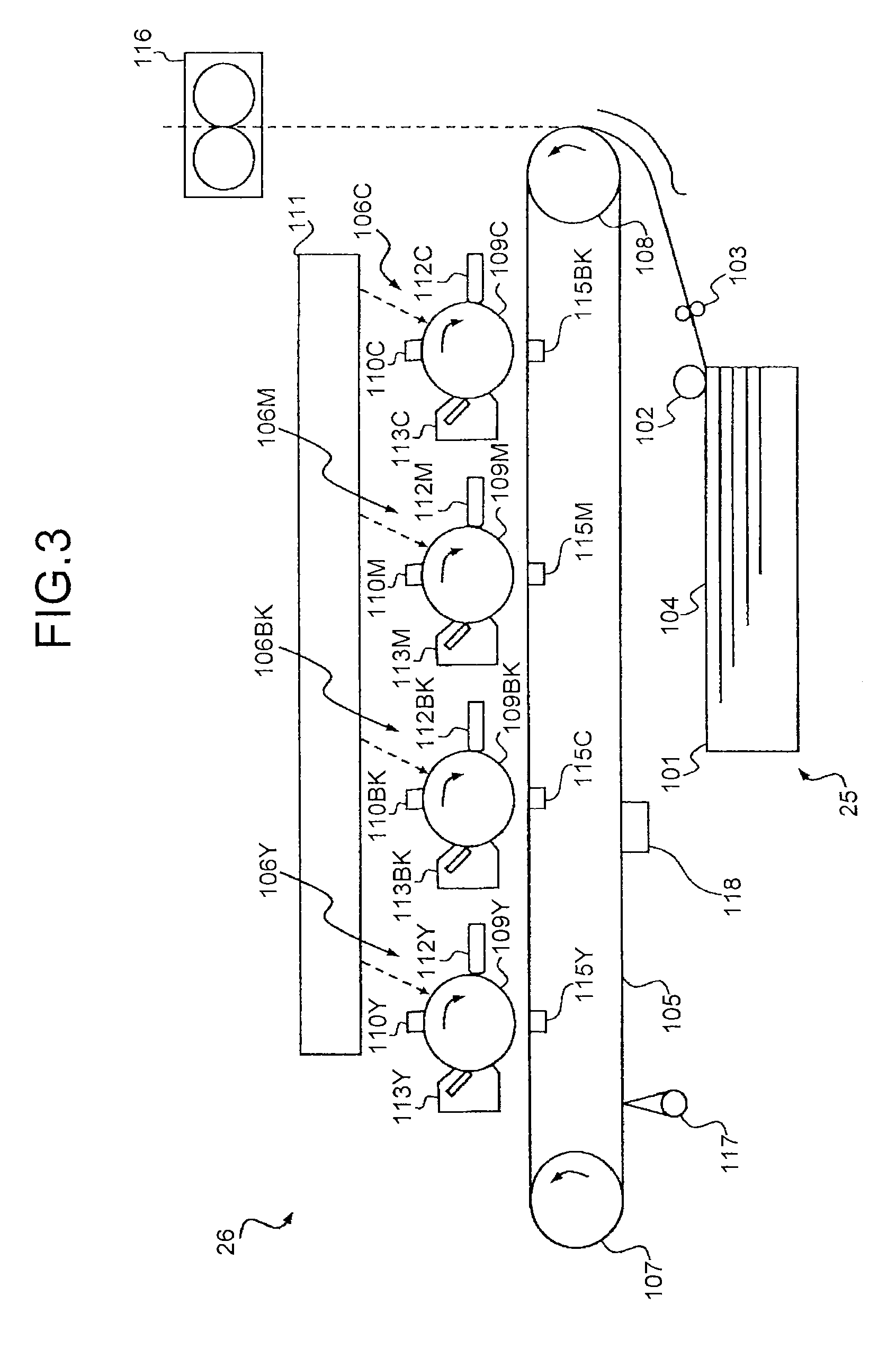
[0040]FIG. 1 is a block diagram illustrating a hardware configuration of an image forming apparatus 1 according to the present embodiment. As illustrated in FIG. 1, the image forming apparatus 1 according to the present embodiment includes an engine for executing image-forming process in addition to the configuration like an information processing terminal such as a generally-available server and PC (Personal Computer). More specificall...


PUM


Abstract

An optical writing control device includes: a light emission control unit which controls light emission of multiple light sources for respective different colors and exposes multiple image carriers; and a correction amount calculating unit which calculates a correction amount for each of the different colors on the basis of a difference between a central value of a distribution range of positional deviation amounts in a sub-scanning direction for the respective different colors and the positional deviation amount for a corresponding color. The light emission control unit delays light emitting timing of a light source, which is to be delayed, by delaying reading timing of pixel information stored in a storage medium, and delays timing at which the pixel information about colors other than a color, light emitting timing of a light source for which is to be advanced, starts to be obtained from an image forming apparatus main body.

Description

CROSS-REFERENCE TO RELATED APPLICATIONS[0001]The present application claims priority to and incorporates by reference the entire contents of Japanese Patent Application No. 2012-148741 filed in Japan on Jul. 2, 2012.BACKGROUND OF THE INVENTION[0002]1. Field of the Invention[0003]The present invention relates to an optical writing control device, an image forming apparatus, and an optical writing control method, and more particularly, the present invention relates to control of light emitting timing of a light source.[0004]2. Description of the Related Art[0005]In recent years, more and more information is made into electronic forms, and image processing apparatuses such as a scanner used to make documents into electronic forms and a printer and a facsimile used to output information made into electronic forms have become essential. Such image processing apparatus includes an image-capturing function, an image-forming function, a communication function, and / or the like, and is often ...

Claims


Application Information

Patent Timeline
Patent Type & Authority Patents(United States)
IPC IPC(8): G06F15/00H04N1/40G03G13/01G03G13/04G03G15/00G03G15/01
CPCG03G13/04G03G13/01G03G15/5058G03G2215/0161G03G15/011
Inventor MIYADERA, TATSUYAKAWANABE, MOTOHIROHAYASHI, MASAYUKISHIRASAKI, YOSHINORIIKEDA, HIROAKIYAMAGUCHI, AKINORIOHSHIMA, TOMOHIRO
Owner RICOH KK
Why Eureka
Try Eureka