Metal gate structure

a metal gate and gate body technology, applied in the direction of semiconductor devices, electrical apparatus, transistors, etc., can solve the problems of reducing the gate capacitance of conventional polysilicon gates, still having many drawbacks of polysilicon devices, and reducing the gate capacitance of conventional polysilicon devices

Active Publication Date: 2014-10-14
UNITED MICROELECTRONICS CORP
View PDF8 Cites 4 Cited by
  • Summary
  • Abstract
  • Description
  • Claims
  • Application Information

AI Technical Summary

Benefits of technology

[0008]It is therefore a primary objective of the present invention to provide a metal gate structure and method of forming the metal gate structure, which has a ratio of nitrogen to titanium (N / Ti) reduced from bottom to top, so as to reduce the EOT, and to maintain the effective work function (EWF).
[0012]Accordingly, the present invention can reduce the EOT of the HK / MG (the high-k dielectric and metal gate) type MOS transistor, and maintains the flat band voltage, and provides a proper EWF value.

Problems solved by technology

However, devices fabricated by polysilicon still have many drawbacks.
On the other hand, the conventional polysilicon gate also has faced problems such as unavoidable depletion effect which increases equivalent thickness of the gate dielectric layer, reduces gate capacitance, and worsens a driving force of the devices.
With a trend towards scaling down the MOS size, conventional methods, which are used to achieve optimization, such as reducing thickness of the gate dielectric layer, for example the thickness of silicon dioxide layer, have faced problems such as leakage current due to tunneling effect.
Accordingly, compatibility and process control for the metal gate are more complicated, meanwhile thickness and composition controls for materials used in the metal gate method have to be more precise.
It is still a challenge to form an optimized work function metal gate to improve the performance of MOS transistors.

Method used


Image

  • Metal gate structure
  • Metal gate structure
  • Metal gate structure

Examples


Embodiment Construction

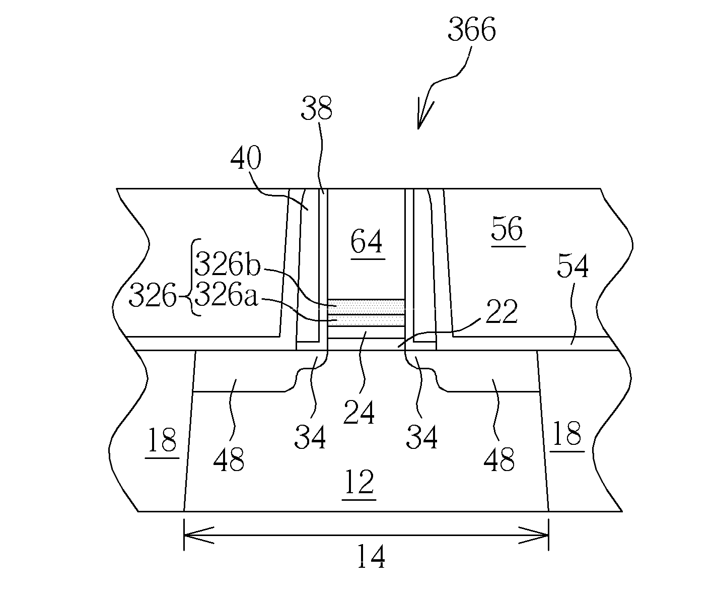
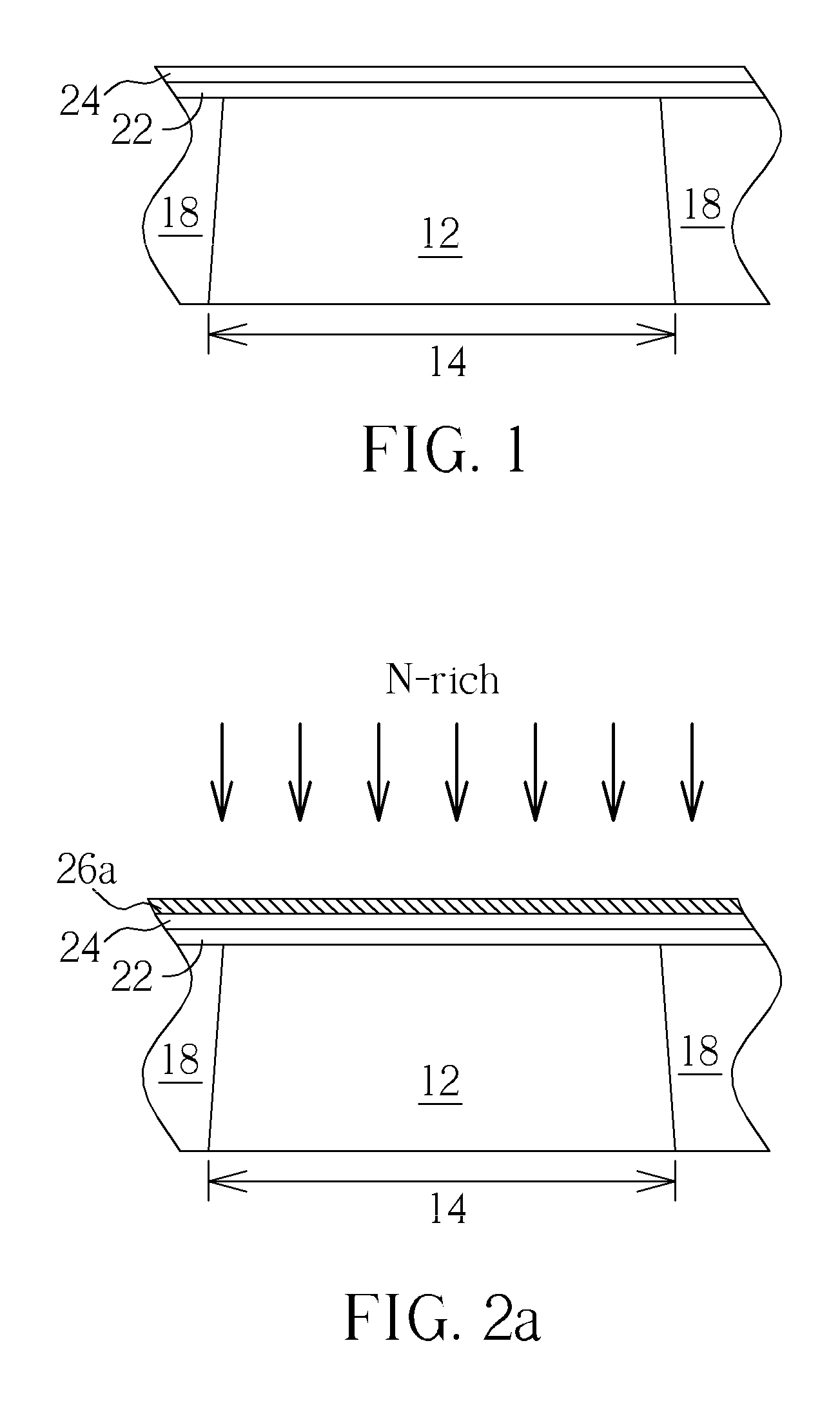
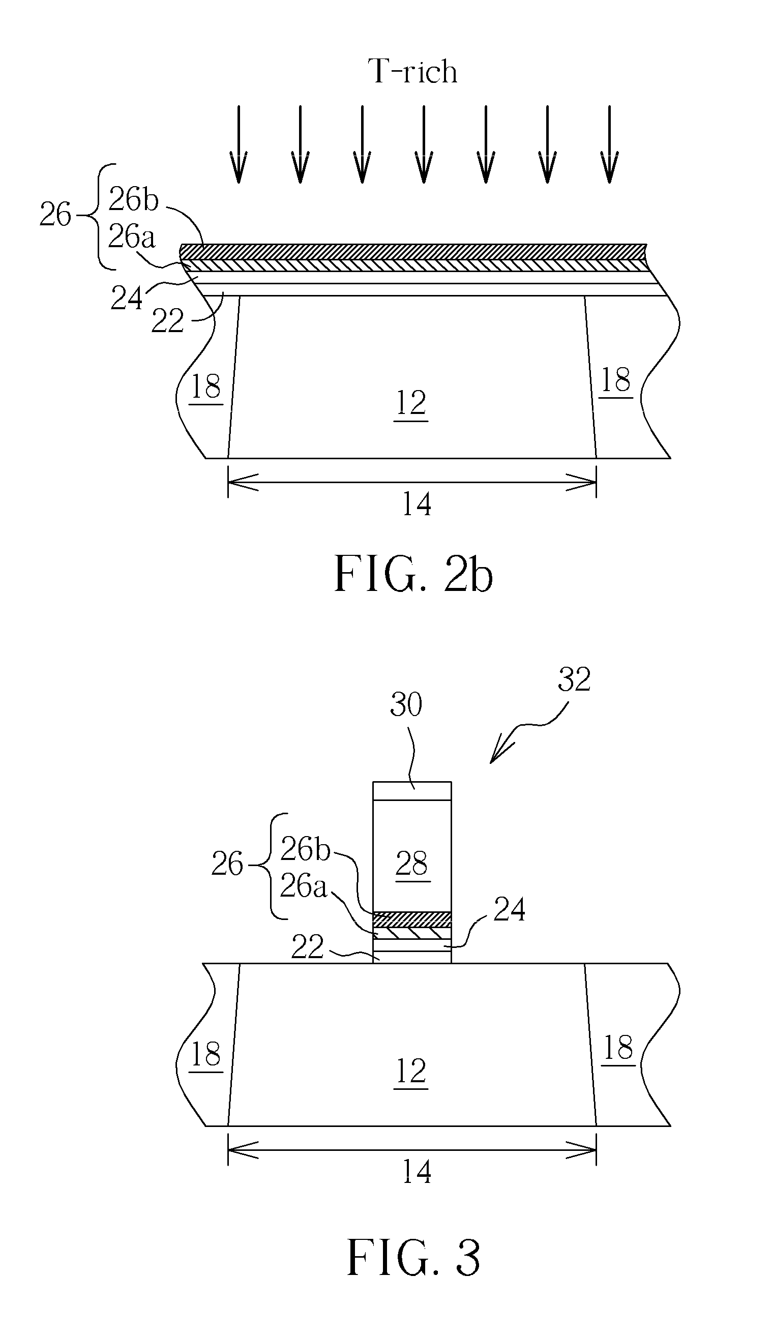
[0018]Hereinafter, preferred embodiments of the present invention will be described in detail with reference to the accompanying drawings. Here, it is to be noted that the present invention is not limited thereto. Furthermore, the step serial numbers concerning the saturation adjustment method are not meant thereto limit the operating sequence, and any rearrangement of the operating sequence for achieving same functionality is still within the spirit and scope of the invention.

[0019]The metal gate structure of the present invention can be a poly-Si / metal stacking gate, or may be consisting essentially of metals, such as a stacking gate including different work function metals. The formation method of the metal gate structure can include depositing a first work function metal layer and a poly-silicon layer, and then patterning the first work function metal layer and the poly-silicon layer by the photo-lithography and etching process to form a gate. In other case, a dummy gate conduct...


PUM

PropertyMeasurementUnit
poweraaaaaaaaaa
poweraaaaaaaaaa
thicknessaaaaaaaaaa

Abstract

The metal gate structure of the present invention can include a TiN complex, and the N / Ti proportion of the TiN complex is decreased from bottom to top. In one embodiment, the TiN complex can include a single TiN layer, which has an N / Ti proportion gradually decreasing from bottom to top. In another embodiment, the TiN complex can include a plurality of TiN layers stacking together. In such a case, the lowest TiN layer has a higher N / Ti proportion than the adjusted TiN layer.

Description

BACKGROUND OF THE INVENTION[0001]1. Field of the Invention[0002]The present invention relates to a metal gate structure and the related manufacture method, and especially to the metal gate of a MOS transistor structure.[0003]2. Description of the Prior Art[0004]In the field of semiconductor fabrication, the use of polysilicon material is diverse. Having a strong resistance for heat, polysilicon materials are commonly used to fabricate gate electrodes for metal-oxide semiconductor transistors. The gate pattern fabricated by polysilicon materials is also used to form self-aligned source / drain regions as polysilicon readily blocks ions from entering the channel region.[0005]However, devices fabricated by polysilicon still have many drawbacks. In contrast to most metal, polysilicon gates are fabricated by semiconductor materials having higher resistance, which causes the polysilicon gate to work under a much lower rate than the metal gates. On the other hand, the conventional polysilico...

Claims


Application Information

Patent Timeline
Patent Type & Authority Patents(United States)
IPC IPC(8): H01L21/70H01L21/28H01L21/8238H01L29/49H01L29/51H01L29/66H01L29/78
CPCH01L29/66545H01L29/7833H01L29/6659H01L21/28088H01L21/823842H01L29/513H01L29/517H01L29/4966
Inventor LIN, CHIN-FUHO, NIEN-TINGLIN, CHUN-HSIENYU, CHIH-HAOCHOU, CHENG-HSIEN
Owner UNITED MICROELECTRONICS CORP
Why Eureka
Try Eureka