Method of forming layered-open-network polishing pads

a technology of open-network and polishing pads, which is applied in the field of polishing pads, can solve the problems of cmp operation being often scratched, gouging or scratching of the wafer, and chatter marks

Active Publication Date: 2014-11-25
DOW GLOBAL TECH LLC
View PDF15 Cites 14 Cited by
  • Summary
  • Abstract
  • Description
  • Claims
  • Application Information

AI Technical Summary

Problems solved by technology

The single greatest problem associated with the CMP operation is often wafer scratching.
Certain polishing pads can interact with foreign materials that result in gouging or scratching of the wafer.
For example, this interaction with foreign material can result in chatter marks in hard materials such as, TEOS dielectrics.
This damage to the dielectric can result in wafer defects and lower wafer yield.
Another scratching issue associated with CMP operations is the damaging of nonferrous interconnects, such as copper interconnects.
If the pad scratches too deep into the interconnect line, the resistance of the line increases to a point where the semiconductor will not function properly.
In extreme cases, polishing creates mega-scratches that can result in the scrapping of an entire wafer.
Although pad manufacturers continue to improve defectivity, industry demands for low defectivity continue to outstrip the state-of-the-art polishing pads.
Although these pads contained solid polymer base layers that facilitate planarization, the pads lacked the compressibility necessary for reducing defects in the most demanding applications.
Furthermore, these pads failed to provide sufficient polishing uniformity for demanding CMP applications.
In particular, the pads were subject to premature failure due to water absorption that resulted in polishing pads having severe dimensional instability.
Although this sounds simple in principle, it often remains a difficult objective.
Alternatively, woven structures can have large surface interactions with substrates surfaces, but these structures often lack a consistent cross-section for uniform polishing.
But the softening of the pad often results in lowered removal rates.

Method used


Image

  • Method of forming layered-open-network polishing pads
  • Method of forming layered-open-network polishing pads
  • Method of forming layered-open-network polishing pads

Examples


example 1

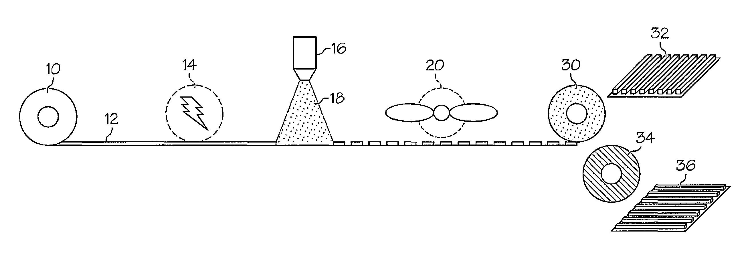
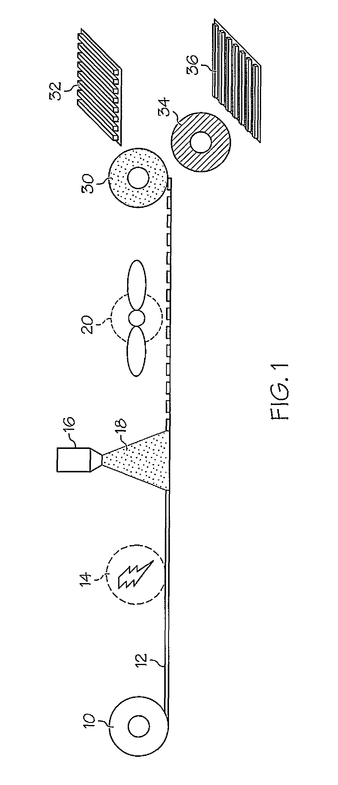
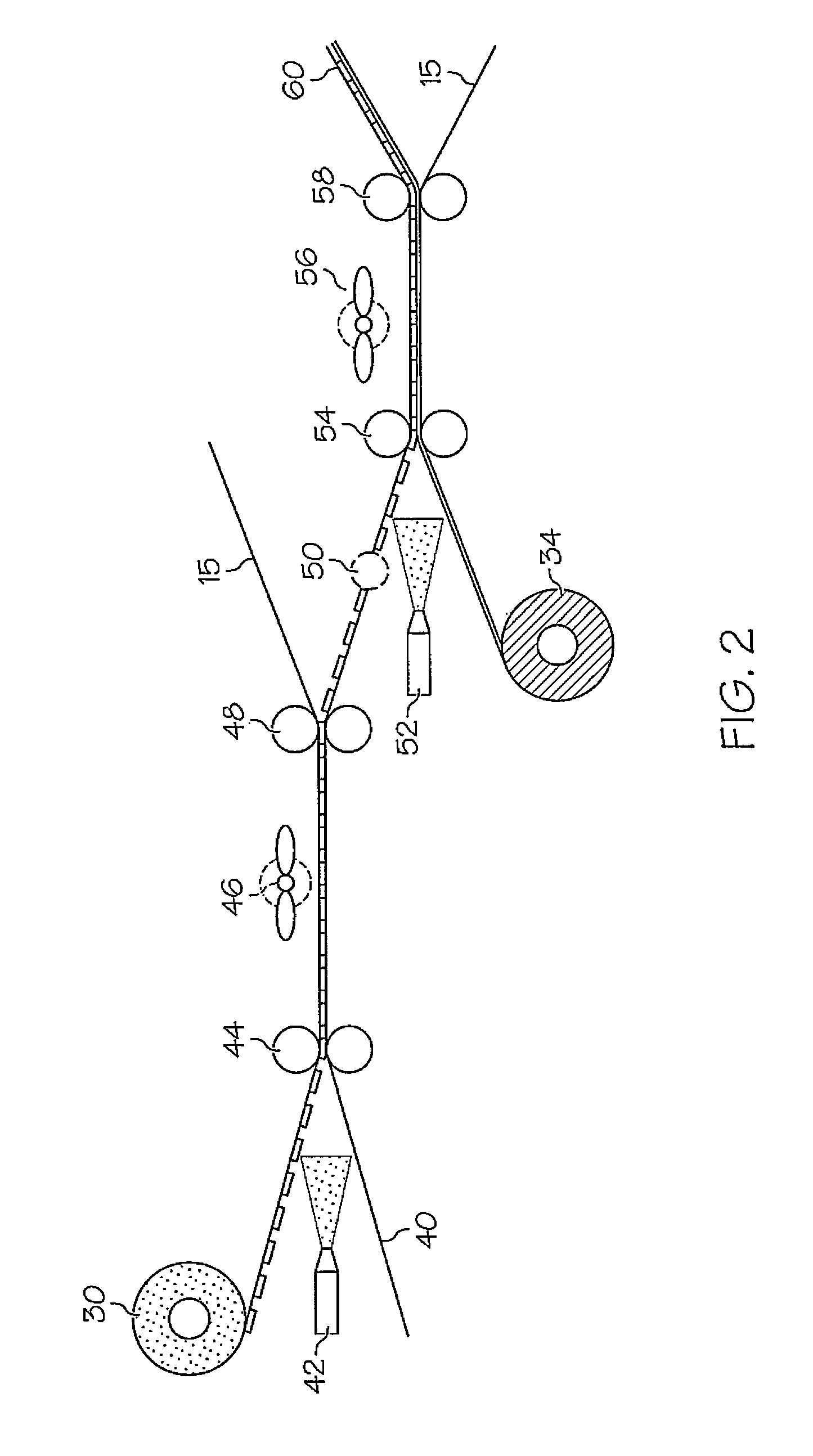
[0045]This Example relates to forming an open-network pad through the use of an open network substrate and a photocurable film. First, stretching a woven polyester fiber 205 mesh (75.5 μm) substrate over an aluminum frame at 20 N / m removes any wrinkles from the substrate. Advantageously, a commercial screen printing degreaser washes and degreases the polyester substrate to remove any dirt or stains. This is important because dirt and stains can prevent good contact between the photocurable film and the woven substrate's polyester fibers. The woven substrate was then wet with clean water with sufficient incline to let excess water run down. Then Ulano photocurable film CDF QT50, as delivered attached to its Mylar polyethylene terephthalate protective sheet, was then rolled out with the unprotected side of the photocurable film towards the exterior. The roll was applied on top of the woven substrate and then unrolled downwards with application of some moderate pressure. This pressure,...

example 2

[0046]This Example relates to forming an open-network pad through the use of adhesive to form an open network substrate. In particular, the method builds up a structured pad by gluing the photocurable polymer film to a woven mesh substrate. A woven polyester fiber 305 mesh (56.6 μm) stretched on an aluminum frame between 15 and 20 N / m removed any wrinkles from the substrate. A commercial screen printing degreaser washed and degreased the polyester substrate to remove dirt and stains. This cleaning step facilitated contact and subsequent adhesion between the woven mesh and the photocurable film. An Ulano CDF QT50 photocurable film (about 60 μm thick) was then placed on top of the woven substrate with edges taped to the polyester woven substrate or to the aluminum frame. A precaution was to tape the rest of the woven substrate to avoid spillage from the next step. The next step was to apply some photoemulsion to one side of the mesh. The photoemulsion puddle was then squeegeed from to...

example 3

[0047]The preparation of the base layer using SaatiChem Thik Film photocurable film of about 100 μm thick was realized as described in Example No. 2 with an exposure time of 120 seconds. The addition of subsequent layers of the photocurable film was done through multiple steps. First, the lamination of the second photocurable film layer required wetting the interface between the photocurable film and the second layer. The most important aspect was to achieve uniform water absorption at the surface of the second photocurable film.

[0048]Water spraying did not provide good enough results, but complete immersion of the photocurable film for an 8 to 10 seconds period in water provided uniform wetting and sufficient absorption for a uniform adhesion of the second photocurable layer. After this wet lamination, the assembly (woven mesh on frame plus two layers) was dried for an hour at 35° C. The protective Mylar polyethylene terephthalate sheet of the second layer was then peeled off and t...


PUM

PropertyMeasurementUnit
temperaturesaaaaaaaaaa
distanceaaaaaaaaaa
rotation angleaaaaaaaaaa

Abstract

The method forms a layered-open-network polishing pad useful for polishing at least one of magnetic, semiconductor and optical substrates. Exposing a first and second polymer sheet or film of a curable polymer to an energy source creates an exposure pattern in the first and second polymer sheet, the exposure pattern having elongated sections exposed to the energy source. Then removing polymer from the exposed first and second polymer sheets to forms elongated channels through the first and second polymer sheets in a channel pattern that corresponds to the exposure pattern. Attaching the first and second polymer sheets forms a polishing pad, the patterns of the first and second polymer sheets cross wherein the first polymer sheet supports the second polymer sheet and the elongated channels from the first and second polymer sheets connect and to form the layered-open-network polishing pad.

Description

BACKGROUND OF THE INVENTION[0001]The present invention relates to polishing pads for chemical mechanical polishing (CMP). In particular relates to methods of forming open-network polishing pads useful for polishing magnetic, optical or semiconductor substrates.[0002]Multi-layer semiconductor wafers having integrated circuits fabricated thereon must be polished to provide a smooth and flat wafer surface. This polishing is necessary to provide a flat surface for subsequent layers and prevent the exaggerated structural distortions that would occur in the absence of polishing. Semiconductor manufacturers accomplish this through multiple CMP operations where a chemical active slurry or abrasive-free polishing solution interacts with a rotating polishing pad to smooth or planarize a wafer's surface.[0003]The single greatest problem associated with the CMP operation is often wafer scratching. Certain polishing pads can interact with foreign materials that result in gouging or scratching of...

Claims


Application Information

Patent Timeline
Patent Type & Authority Patents(United States)
IPC IPC(8): B24D11/00B24B37/26B32B3/10B24B37/22
CPCB24B37/22B24D11/003B24B37/26B24B37/04H01L21/304
Inventor LAKROUT, HAMED
Owner DOW GLOBAL TECH LLC
Why Eureka
Try Eureka