Illumination system

a technology of illumination system and light-emitting device, which is applied in the direction of basic electric elements, electric lighting sources, and light sources that do not continuously emit light, etc., can solve the problems of increasing the power consumption of the external resistor rb>1/b>, easy damage, and inability to continuously emit light, so as to prevent or reduce the flicker effect

Active Publication Date: 2014-11-25
SEOUL VIOSYS CO LTD
View PDF56 Cites 8 Cited by
  • Summary
  • Abstract
  • Description
  • Claims
  • Application Information

AI Technical Summary

Benefits of technology

[0017]An object of the present invention is to provide a light-emitting device for an AC power operation, wherein a flicker effect can be prevented or reduced, and a time during which light is emitted is increased corresponding to a phase change in an AC voltage.
[0018]Another object of the present invention is to provide a light emitting device, wherein an operation can be made with a lower current as compared with a prior art, thereby improving light emitting efficiency.
[0019]To achieve these objects, the present invention provides a light-emitting device for an AC power operation, the device having an array of light emitting cells connected in series. An aspect of the present invention provides a light emitting device, wherein light emitting cells within arrays are sequentially turned on and off. The light emitting device according to the aspect of the present invention comprises a light emitting diode (LED) chip having an array of light emitting cells connected in series; and switching blocks respectively connected to nodes between the light emitting cells. The light emitting cells are sequentially turned on and off by the switching blocks when the array is connected to and driven by an AC voltage power source. Since the light emitting cells are sequentially turned on and off, an effective time during which the light emitting cells emit light can be increased as whole.

Problems solved by technology

Thus, if the LED is used while being connected directly to the AC power source, there is a problem in that it does not continuously emit light and is easily damaged by reverse currents.
However, in this case, power consumption in the external resistor R1 is increased, and a current is also increased according to the increase in the driving voltage.
The increase in a current leads to increase in the junction temperature of the light emitting cells, and the increase in the junction temperature reduces the light emitting efficiency of the light emitting cells.
Even though the effect is not observed with the naked eye, it may cause eye fatigue if the light emitting cells are used for illumination for a long period of time.

Method used


Image

  • Illumination system
  • Illumination system
  • Illumination system

Examples


third embodiment

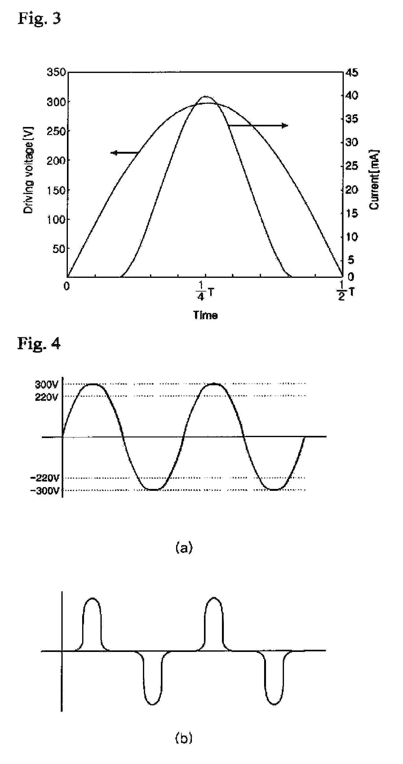
[0140]FIG. 13 is a schematic graph illustrating the operation of the AC light-emitting device according to the present invention. Here, FIG. 13 (a) is waveforms diagram of the AC power source applied to the second node Q2 of the bridge rectifier 400, and FIG. 13 (b) is a graph illustrating a light emission amount of the light emitting device.

[0141]When an AC voltage is applied, a power source with a form in which a reverse voltage is reversed is produced through the rectification operation of the bridge rectifier 400, as shown in FIG. 13 (a). Accordingly, only a forward voltage is applied to the switching block 300. Thus, the arrays 101, 102 and 103 are connected in parallel to each other such that the LED 200 can emit light in response to the forward voltage.

[0142]If the level of a voltage of the AC power source rectified by the bridge rectifier 400 exists in a region A, a current path is formed to the first array 101 by the switching block 300 so that the light emitting cells with...

fourth embodiment

[0144]FIG. 14 is a circuit diagram illustrating an AC light-emitting device according to the present invention. Hereinafter, n represents an integer of 2 or more.

[0145]Referring to FIG. 14, the light emitting device has an LED 200 and additionally, comprises first resistors R1 to Rn and second resistors R′1 to R′n.

[0146]The LED 200 comprises, on a single substrate, a plurality of first arrays A1 to An and a plurality of second arrays RA1 to RAn, each of which has the light emitting cells (30 in FIG. 5) connected in series. The first arrays A1 to An are connected in parallel to each other, and the second arrays RA1 to RAn are connected in reverse parallel to the first arrays.

[0147]The first arrays A1 to An have the different numbers of light emitting cells connected in series. That is, the number of the light emitting cells within the array A1 is smaller than that of the light emitting cells within the array A2, and the number of the light emitting cells within the array A2 is smalle...

fifth embodiment

[0162]FIG. 15 is a schematic circuit diagram illustrating an AC light-emitting device according to the present invention.

[0163]Referring to FIG. 15, the light emitting device has an LED 200 and additionally, has a common resistor Rt. The LED 200 has components that are substantially identical with those of the LED 200 described with reference to FIG. 14.

[0164]In the LED 200, one end portions of the first and second arrays A1 to An and RA1 to RAn may be connected to one another on the substrate 20 in FIG. 5, as described with reference to FIG. 14. Additionally, the other end portions of the first and second arrays may also be connected to one another on the substrate 20 in FIG. 5. The other end portions may be connected to a bonding pad (not shown) provided on the substrate 20 through wires, and the wires may be formed while forming the wires 41 of FIG. 5.

[0165]Meanwhile, instead of the first and second resistors R1 to Rn and R′1 to R′n in FIG. 14, the common resistor Rt is serially ...


PUM


Abstract

An illumination system includes multiple light emitting devices arranged in an area so as to be spaced apart from each other. Each light emitting device includes multiple light emitting diode arrays each of which has one light emitting diode or a plurality of light emitting diodes connected in series. The numbers of the light emitting diodes included in each light emitting diode arrays differs from each other. A controller is configured to establish one or more groups each including one or more light emitting devices and adjust an illumination state of each light emitting device by controlling the driving state of the one or more light emitting diode arrays included in each light emitting device. The controller may select the number of light emitting devices included in each group based on an external condition.

Description

CROSS-REFERENCE TO RELATED APPLICATIONS[0001]The present application is a continuation in part of U.S. patent application Ser. No. 11 / 994,308 filed Dec. 28, 2007, which is the National Stage Entry of International Application No. PCT / KR2006 / 001726, filed on May 9, 2006, and claims priority from and the benefit of Korean Patent Application No. 10-2005-0056175, filed on Jun. 28, 2005; Korean Patent Application No. 10-2005-0104952, filed on Nov. 3, 2005; Korean Patent Application No. 10-2005-0126872, filed on Dec. 21, 2005, Korean Patent Application No. 10-2005-0126873, filed on Dec. 21, 2005, Korean Patent Application No. 10-2005-0126904, filed on Dec. 21, 2005 and Korean Patent Application No. 10-2006-0013322, filed on Feb. 11, 2006, which are all hereby incorporated by reference for all purposes as if fully set forth herein. This application is related to U.S. patent application Ser. No. 12 / 837,805, filed on Jul. 16, 2010, which is a continuation of U.S. patent application Ser. No. ...

Claims


Application Information

Patent Timeline
Patent Type & Authority Patents(United States)
IPC IPC(8): H05B33/08H05B37/02H05B37/00H05B44/00
CPCH05B33/0824H05B37/0245H05B37/0227H01L2224/48137H05B45/44H05B47/175H05B47/14
Inventor LEE, CHUNG, HOON
Owner SEOUL VIOSYS CO LTD
Why Eureka
Try Eureka