
Organic light emitting diode display

a light-emitting diode and organic technology, applied in the direction of discharge tube luminescnet screens, natural mineral layered products, transportation and packaging, etc., can solve the problems of oled display quality degradation, oled display thickness cannot be formed to be slim, etc., and achieve the effect of suppressing moisture permeation

Active Publication Date: 2014-12-02
SAMSUNG DISPLAY CO LTD
View PDF15 Cites 0 Cited by
  • Summary
  • Abstract
  • Description
  • Claims
  • Application Information

AI Technical Summary

Benefits of technology

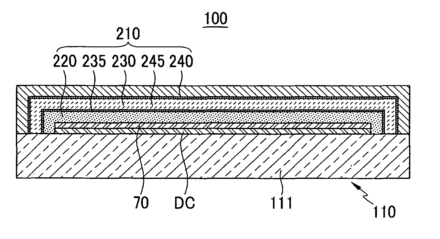
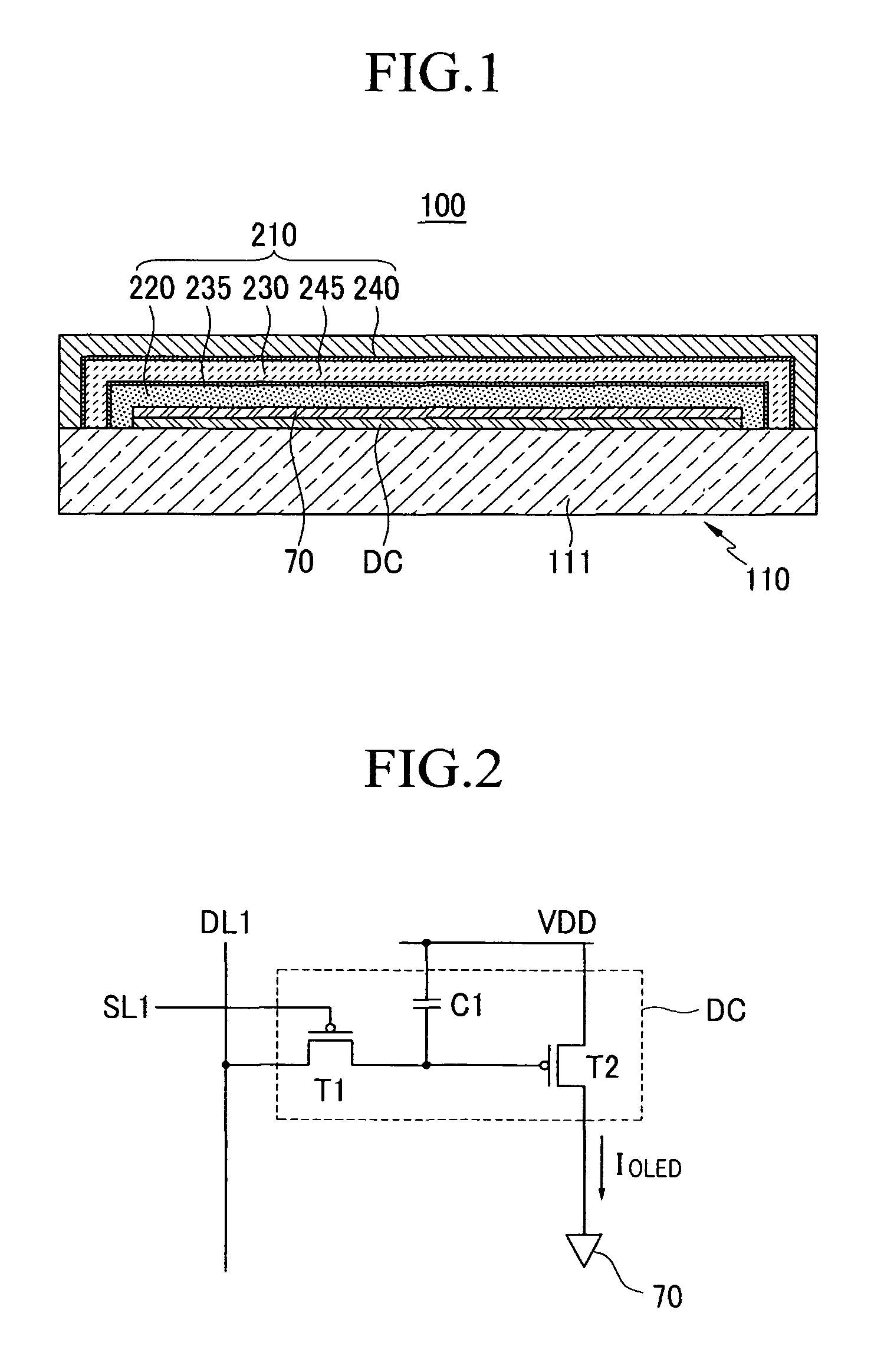
The present invention aims to provide an OLED display that can effectively prevent moisture and oxygen from entering the organic emission layer through a thin film encapsulation layer, while also making the entire device slimmer. Additionally, this invention provides a method for efficiently producing the thin film encapsulation layer.

Problems solved by technology

However, the organic emission layer is sensitive to external environment factors such as moisture and oxygen so that quality of the OLED display may deteriorate when being exposed to the moisture or oxygen.
However, when the encapsulation substrate is used or the protection layer is formed, the manufacturing process of the OLED display becomes complicated to perfectly prevent permeation of the moisture or oxygen into the organic emission layer and the entire thickness of the OLED display cannot be formed to be slim.

Method used


Image

  • Organic light emitting diode display
  • Organic light emitting diode display
  • Organic light emitting diode display

Examples


Embodiment Construction

[0035]The present invention will be described more fully hereinafter with reference to the accompanying drawings, in which exemplary embodiments of the invention are shown. As those skilled in the art would realize, the described embodiments may be modified in various different ways, all without departing from the spirit or scope of the present invention.

[0036]In order to describe the present invention more clearly, parts that are not related to the description will be omitted from the drawings, and the same symbols will be given to similar parts throughout the specification.

[0037]Furthermore, as the size and thickness of the respective structural components shown in the drawings are arbitrarily illustrated for explanatory convenience, the present invention is not necessarily limited to as illustrated.

[0038]In the drawings, the thickness of layers, films, panels, regions, etc., are exaggerated for clarity. It will be understood that when an element such as a layer, film, region, or ...


PUM

PropertyMeasurementUnit
thicknessaaaaaaaaaa
temperatureaaaaaaaaaa
thicknessaaaaaaaaaa

Abstract

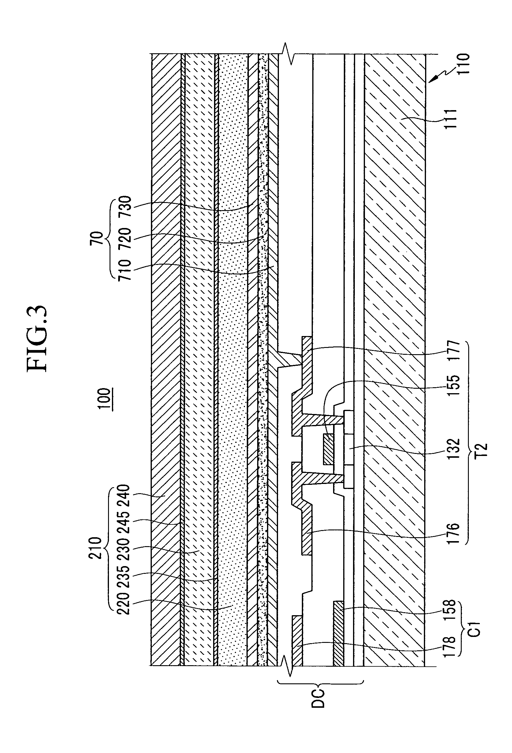
An organic light emitting diode (OLED) display includes a substrate main body, an OLED formed on the substrate main body, a moisture absorbing layer formed on the substrate main body and covering the OLED, a first barrier layer formed on the substrate main body and covering the moisture absorbing layer, a first auxiliary barrier layer formed between the moisture absorbing layer and the first barrier layer, a second barrier layer formed on the substrate main body and covering the first barrier layer, and a second auxiliary barrier layer formed between the first barrier layer and the second barrier layer.

Description

CLAIM OF PRIORITY[0001]This application makes reference to, incorporates the same herein, and claims all benefits accruing under 35 U.S.C. §119 from an application earlier filed in the Korean Intellectual Property Office on 26 Feb. 2009 and there duly assigned Serial No. 10-2009-0016495.BACKGROUND OF THE INVENTION[0002]1. Field of the Invention[0003]The present invention relates to an organic light emitting diode (OLED) display. More particularly, it relates to a thin film encapsulated OLED display.[0004]2. Description of the Related Art[0005]An OLED display has self-luminance characteristics, and the thickness and weight thereof can be reduced since it does not require a separate light source, unlike a liquid crystal display (LCD). In addition, since the OLED display exhibits high-quality characteristics such as low power consumption, high luminance, high response speed, etc., it is receiving much attention as a next-generation display device.[0006]The OLED display includes a plura...

Claims


Application Information

Patent Timeline
Patent Type & Authority Patents(United States)
IPC IPC(8): H01J1/70C23C16/22H01L51/52C23C14/24B32B9/00
CPCH01L51/5237Y10T428/31536Y10T428/2495H10K59/874H10K59/8731H05B33/04H10K50/84H10K50/844H10K50/846H10K50/8445
Inventor SEO, SANG-JOONNAM, KIE HYUN
Owner SAMSUNG DISPLAY CO LTD
Learn More